An audio frequency amplifier or a low frequency amplifier, in order to figure out how it still works and why there are so many different transistors, resistors and capacitors, you need to understand how each element works and try to find out how these elements work. In order to assemble a primitive amplifier, we need three types of electronic elements: resistors, capacitors and of course transistors.
Resistor
So, our resistors are characterized by resistance to electric current and this resistance is measured in Ohms. Each electrically conductive metal or metal alloy has its own specific resistance. If we take a wire of a certain length with high resistivity, then we get a real wirewound resistor. In order for the resistor to be compact, the wire can be wound around the frame. Thus, we get a wirewound resistor, but it has a number of disadvantages, so resistors are usually made of cermet material. This is how resistors are indicated on electrical circuits:The upper designation is adopted in the USA, the lower one in Russia and Europe.
Capacitor
A capacitor consists of two metal plates separated by a dielectric. If we apply a constant voltage to these plates, an electric field will appear, which, after turning off the power, will maintain positive and negative charges on the plates, respectively.
The basis of the design of a capacitor is two conductive plates, between which there is a dielectric
Thus, the capacitor is able to store an electrical charge. This ability to accumulate an electric charge is called electric capacity, which is the main parameter of a capacitor. Capacitance is measured in Farads. What is more characteristic is that when we charge or discharge a capacitor, an electric current flows through it. But as soon as the capacitor is charged, it stops passing electric current, and this is because the capacitor has taken the charge of the power source, that is, the potential of the capacitor and the power source are the same, and if there is no potential difference (voltage), there is no electric current. Thus, a charged capacitor does not pass a direct electric current, but passes an alternating current, since when connected to an alternating electric current, it will constantly be charged and discharged. On electrical diagrams, it is designated as follows:

Transistor
In our amplifier, we will use the simplest bipolar transistors. The transistor is made from a semiconductor material. The property we need is this material - the presence of free carriers of both positive and negative charges. Depending on which charges are more, semiconductors are distinguished into two types by conductivity: n-type and p-type (n-negative, p-positive). Negative charges are electrons released from the outer shells of atoms in the crystal lattice, and positive charges are so-called holes. Holes are vacancies that remain in the electron shells after electrons leave them. Let us conventionally denote atoms with an electron in the outer orbit by a blue circle with a minus sign, and atoms with a vacant place - by an empty circle:
Each bipolar transistor consists of three zones of such semiconductors, these zones are called base, emitter and collector.

Let's look at an example of how a transistor works. To do this, connect two batteries for 1.5 and 5 volts to the transistor, with a plus to the emitter, and a minus to the base and collector, respectively (see the figure):

An electromagnetic field will appear at the contact between the base and the emitter, which literally rips out electrons from the outer orbit of the base atoms and transfers them to the emitter. Free electrons leave holes behind them, and occupy vacant places already in the emitter. The same electromagnetic field has the same effect on the atoms of the collector, and since the base in the transistor is rather thin relative to the emitter and collector, the collector electrons pass through it quite easily into the emitter, and in much larger quantities than from the base.
If we turn off the voltage from the base, then there will be no electromagnetic field, and the base will act as a dielectric, and the transistor will be closed. Thus, by applying a sufficiently low voltage to the base, we can control a higher voltage applied to the emitter and collector.
The transistor we considered pnp-type, since he has two p-zones and one n-zone. There are also npn- transistors, the principle of operation in them is the same, but the electric current flows in them in the opposite direction than in the transistor we have considered. This is how bipolar transistors are indicated on electrical circuits, the arrow indicates the direction of the current: 
ULF
Well, let's try to design a low-frequency amplifier from this all. To begin with, we need a signal that we will amplify, it can be a computer sound card or any other sound device with a line-out. Let's say our signal has a maximum amplitude of about 0.5 volts at a current of 0.2 A, something like this:
And in order for the simplest 4-ohm 10-watt speaker to work, we need to increase the signal amplitude to 6 volts, with a current I = U / R \u003d 6/4 \u003d 1.5 A.
So, let's try to connect our signal to a transistor. Remember our circuit with a transistor and two batteries, now instead of a 1.5 volt battery, we have a line-out signal. Resistor R1 acts as a load so that there is no short circuit and our transistor does not burn out.

But here two problems arise at once, firstly, our transistor npn-type, and opens only when the half-wave is positive, and closes when negative.

Secondly, a transistor, like any semiconductor device, has nonlinear characteristics with respect to voltage and current, and the lower the values \u200b\u200bof current and voltage, the stronger these distortions:

Not only is there only a half-wave left of our signal, it will also be distorted:

This is the so-called crossover distortion.
To get rid of these problems, we need to shift our signal to the working area of \u200b\u200bthe transistor, where the entire sinusoid of the signal will fit and the harmonic distortion will be insignificant. To do this, a bias voltage is applied to the base, say 1 volt, using a voltage divider composed of two resistors R2 and R3.

And our signal entering the transistor will look like this:

Now we need to extract our useful signal from the collector of the transistor. To do this, install capacitor C1:

As we remember, the capacitor passes alternating current and does not pass direct current, so it will serve as a filter for us, passing only our useful signal - our sinusoid. And the constant component that has not passed through the capacitor will be dissipated on the resistor R1. The alternating current, our useful signal, will tend to pass through the capacitor, since the resistance of the capacitor for it is negligible compared to the resistor R1.
So the first transistor stage of our amplifier turned out. But there are two more little nuances:
We do not know 100% what signal enters the amplifier, all of a sudden the signal source is faulty, anything can happen, again, static electricity or a constant voltage passes along with the useful signal. This can cause the transistor to malfunction or even provoke its breakdown. To do this, install the capacitor C2, it, like the capacitor C1, will block direct electric current, and the limited capacitance of the capacitor will not pass large-amplitude peaks that can damage the transistor. These power surges usually occur when the device is turned on or off.

And the second nuance, any signal source requires a certain specific load (resistance). Therefore, the input impedance of the cascade is important for us. To adjust the input resistance, add resistor R4 to the emitter circuit:

We now know the purpose of each resistor and capacitor in the transistor stage. Let's now try to calculate what element denominations you need to use for it.
Initial data:
- U \u003d 12 V - supply voltage;
- U bae ~ 1 V - Voltage emitter-base of the operating point of the transistor;

- P max \u003d 200 mW - maximum power dissipation;
- I max \u003d 100 mA - maximum constant collector current;
- U max \u003d 18 V - the maximum allowable collector-base / collector-emitter voltage (We have a supply voltage of 12 V, so there is enough with a margin);
- U eb \u003d 5 V - the maximum allowable emitter-base voltage (our voltage is 1 volt ± 0.5 volts);
- h21 \u003d 75-225 - base current amplification factor, the minimum value is taken - 75;
- We calculate the maximum static power of the transistor, it is taken 20% less than the maximum dissipated power, so that our transistor does not work at the limit of its capabilities:
P article max = 0,8*P max \u003d 0.8 * 200mW \u003d 160mW;
- Determine the collector current in a static mode (without a signal), despite the fact that no voltage is supplied to the base through the transistor, an electric current still flows to a small extent.
I k0 = P article max / U kewhere U ke - voltage of the collector-emitter junction. Half of the supply voltage is dissipated on the transistor, the second half will be dissipated on resistors:
U ke = U / 2;
I k0 = P article max / (U / 2) \u003d 160 mW / (12V / 2) \u003d 26.7 mA;
- Now let's calculate the load resistance, initially we had one resistor R1, which played this role, but since we added a resistor R4 to increase the input resistance of the stage, now the load resistance will be the sum of R1 and R4:
R n = R1 + R4where R n - total load resistance;
The ratio between R1 and R4 is usually 1 to 10:
R1 = R4*10;
Let's calculate the load resistance:
R1 + R4 = (U / 2) / I k0 \u003d (12V / 2) / 26.7 mA \u003d (12V / 2) / 0.0267 A \u003d 224.7 Ohm;
The closest resistors are 200 and 27 ohms. R1 \u003d 200 Ohm, and R4 \u003d 27 ohms.
- Now let's find the voltage at the collector of the transistor without a signal:
U k0 = (U ke0 + I k0 * R4) = (U - I k0 * R1) \u003d (12V -0.0267 A * 200 Ohm) \u003d 6.7 V;
- Transistor control base current:
I b = I to / h21where I to - collector current;
I to = (U / R n);
I b = (U / R n) / h21 \u003d (12V / (200 Ohm + 27 Ohm)) / 75 \u003d 0.0007 A \u003d 0.07 mA;
- The total base current is determined by the base bias voltage, which is set by the divider R2 and R3... The current set by the divider must be 5-10 times greater than the base control current ( I b) so that the actual base control current does not affect the bias voltage. Thus, for the divider current value ( I cases) we take 0.7 mA and calculate R2 and R3:
R2 + R3 = U / I cases \u003d 12V / 0.007 \u003d 1714.3 Ohm
- Now let's calculate the voltage at the emitter at rest of the transistor ( U uh):
U uh = I k0 * R4 \u003d 0.0267 A * 27 Ohm \u003d 0.72 V
Yes, I k0 the quiescent current of the collector, but the same current passes through the emitter, so that I k0 consider the quiescent current of the entire transistor.
- We calculate the total voltage at the base ( U b) taking into account the bias voltage ( U cm \u003d 1B):
U b = U uh + U cm \u003d 0.72 + 1 \u003d 1.72V
Now, using the voltage divider formula, we find the values \u200b\u200bof the resistors R2 and R3:
R3 = (R2 + R3) * U b / U \u003d 1714.3 Ohm * 1.72 V / 12 V \u003d 245.7 Ohm;
The closest resistor rating is 250 Ohm;
R2 = (R2 + R3) - R3 \u003d 1714.3 Ohm - 250 Ohm \u003d 1464.3 Ohm;
We select the resistor value in the direction of decreasing, the closest R2 \u003d 1.3 kΩ.
- Capacitors C1 and C2 usually set at least 5 μF. The capacity is chosen so that the capacitor does not have time to recharge.
Conclusion
At the output of the stage, we get a proportionally amplified signal in terms of both current and voltage, that is, in terms of power. But one stage is not enough for the required amplification, so we have to add the next and the next ... And so on.The considered calculation is rather superficial and of course such an amplification scheme is not used in the structure of amplifiers, we should not forget about the range of pass frequencies, distortions and much more.
The quantitative characteristics of these requirements are different for the RF amplifier of different ranges. In this case, unstable operation means changes in the main parameters and characteristics of the amplifier up to the transition to the self-excitation mode in time under the influence of various destabilizing factors. fig. Part of this voltage through the supply circuits penetrates into the previous stages, in particular into their input circuits through the elements ...
Share your work on social media
If this work did not suit you at the bottom of the page there is a list of similar works. You can also use the search button
LECTURE 5
- RF Amplifiers and Low Noise Amplifiers
2.4.1 Overview of RF Amplifiers
A radio frequency amplifier (selective) refers to amplifiers that use frequency selective circuits as a load, as a result of which the gain also becomes frequency dependent. In the simplest case, an oscillatory circuit is used as such a circuit. DUTs are designed to ensure high sensitivity of the radio control system due to preliminary amplification of the radio signal and its selection against the background of interference. The use of resonant systems is necessary to ensure the required selectivity of the receiver in the mirror and direct reception channels.
The main quality indicators of selective amplifiers are:
- Resonant voltage gain;
- Selectivity by side channels of reception;
- Noise figure;
- Dynamic range.
Here is the maximum input voltage at which the nonlinear distortions still do not exceed the permissible value; - input voltage, at which the required S / N ratio is provided at the amplifier output.
Due to the tasks they solve, the following requirements are imposed on the URCH:
Providing frequency selectivity for additional reception channels (direct, mirror, combinational);
Ensuring the required noise figure;
Ensuring the required stable gain required to bring the level of the received signals to the value required for the normal operation of subsequent stages.
The quantitative characteristics of these requirements are different for the RF amplifier of different ranges. As you know, in the LW, MW and HF ranges, the sensitivity is determined by the level of external noise entering the receiver input. Under these conditions, a high gain is not required, so usually no more than two stages with a common K are used.0 \u003d 2 ... 5. The main attention is paid to ensuring selectivity in the forward and mirror receiving channels, as well as ensuring high linearity of the cascades to exclude the occurrence of combination receiving channels and intermodulation distortions.
One and two-circuit systems are used as a load, since more complex ones make it difficult to rebuild along the range. Preference is given to the use of MOSFETs, which provide the best linearity of the stages.
In the UHF ranges and higher, the sensitivity is determined by its own noise. It is very important here to ensure the required noise figure. The sensitivity of receivers in these ranges can reach a few microvolts, so a large gain is required in the input stages. Usually used 1 ... 3 stages with a common K0 \u003d 100 ... 200, often non-tunable, since the values \u200b\u200bof the intermediate frequency in this case are chosen high enough and suppression of side reception channels in the entire received range is easily ensured. Tunnel diode amplifiers and parametric amplifiers can be used to reduce noise figure.
2.4.2 Connection diagrams of active elements


2.4.3 Stability and self-excitation of the RF amplifier
A) Factors affecting sustainability
As is known, with a PIC, the amplifier gain is described by the expression
, (3.1)
where is the transmission coefficient of the feedback circuit. The product is called the loop gain stage. According to the Nyquist criterion, the cascade is on the threshold of generation (self-excitation) under the condition \u003d 1, or, which is the same,
(3.2)
This condition splits into two
1) , (3.3)
those. the total phase incursion along the path from the amplifier input to the output and back must be a multiple of 2 (the so-called phase balance);
2) =1, (3.4)
those. the part of the signal that goes back to the input of the amplifier must be equal to the original signal (amplitude balance).

Figure 3.2 providing a constant current mode (U os on the picture). Under certain conditions, this feedback can be positive.
To eliminate feedback of this type, the power source is shunted by an alternating current with a large capacitor and filters are used in the power circuits of individual stages (Figure 3.3).

Filter resistancesR f chosen equal to 1 ... 3 kOhm. Filter capacitors - from the condition. Ceramic capacitors must be used, since film and electrolytic capacitors have a high intrinsic inductance due to the fact that they are structurally made in the form of rolls containing a large amount of vit-
Figure 3.3 cov. Capacitors are installed in the immediate vicinity of the load oscillating circuits in order to shorten the path of high frequency currents.
2. Capacitive coupling between the output and the input of one stage or between stages. Obviously, any two conductors that are at some distance from each other can be considered a capacitor. So, for example, the terminals of a transistor with a length of about a centimeter can have a capacity in the range of 1 ... 10 pF, depending on their relative position. At high frequencies, this is a very noticeable value.
3. Inductive coupling between input and output of one stage or between stages.
To reduce it, magnetic shields are used (armor cores made of ferrites, carbonyl iron, etc.), minimizing the length of the leads and connecting conductors. The input and output coils are placed at the greatest possible distance from each other, orienting their longitudinal axes in mutually perpendicular planes to reduce mutual inductances.
By choosing the right means, all of the above reasons for the occurrence of POS can be partially or completely eliminated. However, there is always one more channel for the penetration of a part of the output signal to the input - the internal conductance of the feedback of the active element.Y 12 ... In any real amplifying device, it is nonzero and cannot be eliminated. Its effect can only be compensated up to certain limits.
B) Conditions for the absence of self-excitation in the selective amplifier
Let us consider for simplicity the situation when the signal source for the selective amplifier and its load are exactly the same stages (Figure 3.4). In this case, the cascade parameters of the same name are the same:
I. (3.5)

Having recalculated the output conductivity of the previous stage, first into the circuit, and then directly to the input of the transistor, we get the resulting conductivity connected to the input (Figure 3.5):. (3.6)
Figure 3.4
Similarly, the input conductivity of the next stage, reduced to the output of the transistor, will be written as:
. (3.7)
Please note thatU in Fig. 3.4 and U 1 in Figure 3.5 are different quantities, as well asU out and U 2.

For further analysis, it is necessary to obtain expressions describing the gain of the amplifier in the absence of feedback () and the gain of the feedback loop (). For this purpose, replace the transistor in the previous
Figure 3.5 diagram for its equivalent, assuming that there is no feedback conduction in it. The converted circuit is shown in Figure 3.6.

The voltage transfer coefficient of such a circuit is determined by the expression:. (3.9)
Note that it is not equal to the coefficient
Figure 3.6 the gain of the original (Figure 3.4) amplifier, which is determined by the expression:
. (3.10)
From the circuit (Figure 3.6), it is obvious that the output voltage can be obtained by dividing the output current by the resulting output conductance:
. (3.11)
The minus sign in the expression takes into account the opposite direction of current flow through the conduction and the voltage across them.
Substituting the right side of this expression into the numerator of formula (3.9) and reducing the fraction by, we get:
. (3.12)
Similar reasoning allows one to derive an expression for. The reason for the appearance of the feedback voltage () at the input of the amplifier is the output voltage of the transistor and the conductance of the feedback. Excluding from consideration the passage of the signal through the amplifier in the forward direction, i.e. assuming \u003d 0, its equivalent circuit for transmitting the feedback signal can be represented in the form shown in Fig. 3.7.

Under the influence of the output voltage, a current will flow through the input conductances (see Figure 3.7), creating a voltage drop across them:
. (3.13)
Figure 3.7
The transmission coefficient of the feedback circuit is determined by the formula, substituting the right side of expression (3.13) into its numerator:
. (3.14)
The formula for the loop gain is obtained by multiplying the right-hand sides of expressions (3.14) and (3.12):
. (3.15)
Instead of conductivities and, we substitute the right-hand sides of formulas (3.6) and (3.7) in the denominator of the last expression, respectively:
. (3.16)
The expression in the denominator in parentheses represents the equivalent conductivity of the load circuit of the selective amplifier with the conductivities of the previous and subsequent stages recalculated into it (see formula ()) and can be represented as. Taking this into account, finally, formula (3.16) can be rewritten as:
. (3.17)
B) Phase and amplitude balance
When designing selective amplifiers with the proper choice of transistor, it is usually easy to satisfy the condition that the cutoff frequency of the gain of the transistor is at least three times the maximum operating frequency of the amplifier. In this case, the complex conductance of the direct transmission can be considered purely active, i.e. ... The conductivity of the feedback, on the contrary, is purely imaginary and formed by the internal (through-flow) capacity (C12 ) connecting the output and input regionsp - n transitions of the transistor (for the OE circuit, this is the capacitance of the collector-base junction, for example. The active conductivity of the reverse-biased collector junction is negligible in this case). In other words, you can write: We take these changes into account in (3.17) and multiply the numerator and denominator by.
. (3.18)
The components of the formula in curly brackets represent the square of the resonant gain of the amplifier (see formula ()). Having made the appropriate replacement, we get:
. (3.19)
We multiply the numerator and denominator by the value complexly conjugated with the one in the denominator, and select the real and imaginary parts in the resulting expression in explicit form:
(3.20)
The resulting expression allows one to analyze the conditions for the occurrence of self-excitation in the amplifier. The phase balance, in accordance with (3.3), means that the coefficient at the imaginary part of formula (3.20) is zero:
. (3.21)
It is known that the fraction is zero when the numerator is zero, i.e. \u003d 0. The first three factors here cannot be zero, therefore \u003d 0, or \u003d 1. The latter is possible in two cases:
; (3.22)
. (3.23)
The generalized detuning is equal to unity, as is known, at the boundaries of the amplifier passband.Only at these points is the phase balance performed and self-excitation of the amplifier is possible!
The obtained condition is necessary, but not sufficient. The amplitude balance condition, in accordance with formulas (3.4) and (3.20), means:
1. (3.24)
Since there is a positive value on the right side of the equality, then the left side must also be positive. This is possible only when \u003d -1, since the other components of the formula cannot be negative. This limitationmeans that self-excitation is possible only at the left edge of the amplifier's bandwidth.
The considered conditions of self-excitation allow us to conclude that to ensure stable operation of the amplifier, it is necessary that the left side of equation (3.24) be less than unity. Moreover, the stronger this inequality, the more stable the amplifier. For a quantitative assessment of stability, the concept of stability coefficient γ is introduced, defining it as
. (3.25)
Obviously, for γ \u003d 1, there is no feedback in the cascade (the left-hand side of equation (3.4) is zero) and the amplifier is absolutely stable, and for γ \u003d 0 the self-excitation conditions are satisfied and the amplifier turns into a generator.
In practice, the required value of γ is usually set. Taking it into account, we obtain the stability condition for the cascade from formula (3.4):
. (3.26)
Substituting into this expression the value of the left side from (3.24) and putting ξ \u003d -1, we get:
. (3.27)
Since the stability conditions are provided on the right side, the value of K0 on the left - there is a value at which the amplifier is stable. We denote this value through and express it from (3.27) in an explicit form:
Or (3.28)
In practice, choose γ \u003d 0.8 ... 0.9. For γ \u003d 0.9, the formula takes the form:
. (3.29)
For a circuit with an OE, for example, the formula takes on a form suitable for practical calculations
. (3.30)
It can be seen from the formula that to increase the stable gain, it is necessary to choose a transistor with a large value of the current transfer coefficienth 21 , low AC input impedanceh 11 and the lowest possible value of the throughput capacity C12 .
It should be emphasized that in any case, in the presence of a PIC, even if self-excitation is absent, the frequency response of the amplifier is distorted. The stronger the feedback (the more), the more distorted the shape of the resonance characteristic (Figure 3.8).

Figure 3.8
In conclusion, it should be noted that many simplifications were used to increase the "transparency" of the reasoning. In real amplifiers, the picture is much more complicated, however, the main causes and patterns of self-excitation are the same.
Other similar works that may interest you. Wshm\u003e |
|||
| 6657. | AMPLIFIERS AND GENERATORS ON TRANSISTORS | 44.93 KB | |
| Electric signal amplifiers are devices for amplifying it in terms of voltage, current or power by converting the energy of the power source into the energy of the output signal. The amplifiers have an input circuit to which the source of the amplified signal is connected; the output circuit to which the load consumer of the amplified signal is connected, as well as the power circuit to which the source is connected, due to the energy of which the signal is amplified. The nature of the amplified signal is determined by its source ... | |||
| 11950. | Bismuth fiber lasers and birefringent fiber amplifiers with polarized output radiation for telecommunication systems | 152.45 KB | |
| A brief description of the development. Development advantages and comparison with foreign counterparts. The main development advantage lies in obtaining new lasing wavelengths in active optical fibers. Development implementation form. | |||
To increase the sensitivity and real selectivity of the heterodyne receiver, the input circuit should provide a power transfer coefficient close to unity in the operating frequency range and the maximum possible attenuation of out-of-band signals. All these are properties of an ideal band-pass filter, therefore, the input circuit must be performed in the form of a filter.
The frequently used single-loop input circuit is the worst suited to the requirements. To increase selectivity, it is necessary to increase the loaded Q-factor of the circuit, weakening its connection with the antenna and mixer or RF amplifier.
But then almost all the power of the received signal will be consumed in the circuit and only a small part of it will go to the mixer or RF amplifier. The power transmission ratio will be low. If, however, the loop is strongly connected to the antenna and mixer, the loaded Q-factor of the loop will drop and it will slightly attenuate the signals of neighboring stations in frequency.
But very powerful radio broadcasting stations work next to the amateur bands.
A single input circuit as a preselector can be used in the low-frequency HF bands, where the signal levels are high enough, in the simplest heterodyne receivers. The connection with the antenna should be made adjustable, and the circuit itself should be tunable, as shown in Fig. one.
In the case of interference from powerful stations, it is possible to weaken the connection with the antenna, reducing the capacitance of the capacitor C1, thereby increasing the selectivity of the circuit and at the same time increasing the losses in it, which is equivalent to turning on the attenuator. The total capacitance of capacitors C2 and C3 is chosen about 300 ... 700 pF, these coils depend on the range.
Fig. 1. Single-circuit input circuit.
Significantly better results are obtained with bandpass filters matched in input and output. In recent years, there has been a tendency to use switchable bandpass filters even at the input of wide-range professional communications receivers. Octave (rarely), half-octave and quarter-octave filters are used.
The ratio of the upper frequency of their passband to the lower one is respectively 2; 1.41 (root of 2) and 1.19 (fourth root of 2). Of course, the narrower the input filters, the higher the noise immunity of a wide-range receiver, but the number of switchable filters increases significantly.
For receivers designed for amateur bands only, the number of input filters is equal to the number of bands, and their bandwidth is chosen equal to the bandwidth, usually with a margin of 10 ... 30%.
In transceivers it is advisable to install bandpass filters between the antenna and the antenna transmit / receive switch. If the transceiver's power amplifier is wide enough, such as in the case of a transistor amplifier, its output can contain many harmonics and other out-of-band signals. A bandpass filter will help to suppress them.
The requirement of close to unity of the filter power transmission coefficient is especially important in this case. The filter elements must withstand a reactive power several times the nominal power of the transceiver transmitter.
It is advisable to select the characteristic impedance of all range filters to be the same and equal to the characteristic impedance of the 50 or 75 Ohm feeder.

Fig. 2. Bandpass filters: a - L-shaped; b - U-shaped
The classical scheme of the L-shaped bandpass filter is shown in Fig. 2, a. Its calculation is extremely simple. First, the equivalent quality factor Q \u003d fo / 2Df is determined, where fo is the middle frequency of the range, 2Df is the filter bandwidth. The inductances and capacities of the filter are found by the formulas:
where R is the characteristic impedance of the filter.
At the input and output, the filter must be loaded with resistances equal to the characteristic, they can be the input impedance of the receiver (or the output transmitter) and the antenna impedance.
The mismatch up to 10 ... 20% practically has little effect on the characteristics of the filter, but the difference between the load resistances from the characteristic one dramatically distorts the selectivity curve several times, mainly in the passband.
If the load resistance is less than the characteristic one, it can be connected autotransformer, to the L2 coil tap. The resistance will decrease k2 times, where k is the switching coefficient equal to the ratio of the number of turns from the tap to the common wire to the total number of turns of the L2 coil.
The selectivity of one L-shaped link may be insufficient, then the two links are connected in series. The links can be connected either in parallel branches to each other, or in series. In the first case, a T-shaped filter is obtained, in the second - a U-shaped one.
Elements L and C of the connected branches are combined. As an example, Fig. 2, b shows a U-shaped bandpass filter. Elements L2C2 remained the same, and elements of longitudinal branches were combined into inductance 2L and capacitance C1 / 2. It is easy to see that the tuning frequency of the resulting serial circuit (as well as the other filter circuits) remained the same and equal to the center frequency of the range.
Often, when calculating narrow-band filters, the value of the capacitance of the longitudinal branch C1 / 2 turns out to be too small, and the inductance too large. In this case, the longitudinal branch can be connected to the taps of the L2 coils, increasing the capacitance by 1 / k2 times, and reducing the inductance by the same amount.
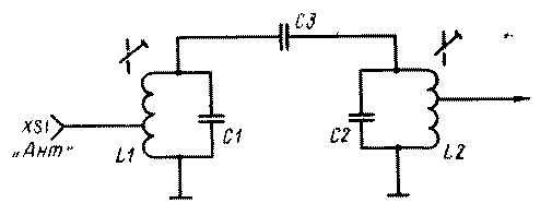
Fig. 3. Dual-circuit filter.
It is convenient to use only parallel oscillatory circuits with single-ended filters with a common wire.
The circuit of a dual-loop filter with external capacitive coupling is shown in Fig. 3. The inductance and capacitance of parallel circuits are calculated by formulas (1) for L2 and C2, and the capacitance of the coupling capacitor should be C3 \u003d C2 / Q.
The switching factors of the filter outputs depend on the required input resistance Rin and the characteristic resistance of the filter R: k2 \u003d Rin / R. The inclusion coefficients on both sides of the filter can be different, providing matching with the antenna and the receiver input or transmitter output.
To increase the selectivity, three or more identical circuits can be switched on according to the scheme in Fig. 3, reducing the capacitance of the coupling capacitors SZ by 1.4 times.
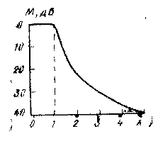
Fig. 4. Three-loop filter selectivity.
The theoretical curve of selectivity of a three-loop filter is shown in Fig. 4. The horizontal is the relative detuning x \u003d 2DfQ / fo, and the vertical is the attenuation introduced by the filter.
In the transparency band (x<1) ослабление равно нулю, а коэффициент передачи мощности - единице. Это понятно, если учесть, что теоретическая кривая построена для элементов без потерь, имеющих бесконечную конструктивную добротность.
A real filter introduces some attenuation in the passband, which is associated with losses in the filter elements, mainly in the coils. The filter loss decreases with an increase in the constructive Q-factor of the coils Q0. For example, at Q0 \u003d 20Q, the loss even in a three-loop filter does not exceed 1 dB.
Out-of-band attenuation is directly related to the number of filter loops. For a double-loop filter, the attenuation is 2/3 indicated in Fig. 4, and for a single-loop input circuit, it is 1/3. For the U-shaped filter in Fig. 3, b, the selectivity curve in Fig. 4 is suitable without any correction.

Fig. 5. A three-loop filter is a practical design.
A practical diagram of a three-loop filter with a bandwidth of 7.0 ... 7.5 MHz and its experimentally measured characteristic are shown in Figs. 5 and 6, respectively.
The filter is calculated according to the described method for resistance R \u003d 1.3 kΩ, but it was loaded on the input impedance of the mixer of the heterodyne receiver of 2 kΩ. Selectivity increased slightly, but peaks and dips appeared in the bandwidth.
The filter coils are wound turn to turn on frames with a diameter of 10 mm with a PEL 0.8 wire and contain 10 turns each. The L1 coil is tapped to match the 75 Ohm antenna feeder resistance from the second turn.
All three coils are enclosed in separate screens (aluminum cylindrical "cups" from nine-pin lamp panels). Tuning the filter is simple and boils down to tuning the contours to resonance with the coil trimmers.
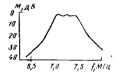
Fig. 6. The measured selectivity curve of a three-loop filter.
Special attention should be paid to the issues of obtaining the maximum constructive Q-factor of the filter coils. One should not strive for special miniaturization, since the figure of merit increases with an increase in the geometric dimensions of the coil.
For the same reason, it is undesirable to use a wire that is too thin. Silver plating of the wire has a noticeable effect only on high-frequency KB bands and on VHF with a constructive quality factor of the coil over 100. It is advisable to use the litz wire only for winding coils in the 160 and 80 m ranges.
Smaller losses in the silver-plated wire and litz wire are due to the fact that high-frequency currents do not penetrate into the thickness of the metal, but flow only in a thin surface layer of the wire (the so-called skin effect).
A perfectly conductive screen does not reduce the Q-factor of the coil and also eliminates energy losses in the objects surrounding the coil. Real screens introduce some losses, so it is advisable to choose the screen diameter equal to at least 2-3 coil diameters.
The screen should be made of a highly conductive material (copper, slightly worse aluminum). Painting or tinning of the inner surfaces of the screen is inadmissible.
These measures provide an exceptionally high Q-factor of the coils, which is realized, for example, in spiral resonators.
In the 144 MHz range, it can reach 700 ... 1000. Figure 7 shows the design of a 144 MHz dual-cavity bandpass filter designed to be plugged into a 75-ohm feed line.
The resonators are mounted in rectangular screens 25X25X50 mm in size, soldered from sheet copper, brass or double-sided foil-clad fiberglass plates.
The inner baffle has a 6X12.5 mm tie hole. Air trimmer capacitors are fixed on one of the end walls, the rotors of which are connected to the screen.
The resonator coils are frameless. They are made of silver-plated wire with a diameter of 1.5 ... 2 mm and have 6 turns with a diameter of 15 mm, evenly stretched to a length of about 35 mm. One lead of the coil is soldered to the stator of the trimmer capacitor, the other to the screen.
Taps to the filter inlet and outlet are made from 0.5 turns of each cog. The bandwidth of the tuned filter is slightly more than 2 MHz, the insertion loss is calculated in tenths of a decibel. The bandwidth of the filter can be adjusted by changing the dimensions of the coupling hole and selecting the position of the coil taps.
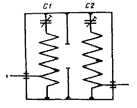
Fig. 7. Spiral resonator filter.
At higher VHF frequencies, it is advisable to replace the coil with a straight piece of wire or tube, then the spiral resonator turns into a coaxial quarter-wave resonator loaded with a capacitance.
The length of the resonator can be chosen about l / 8, and the length that is missing up to a quarter of the wavelength is compensated for by the tuning capacitance.
In especially difficult reception conditions on the KB bands, the input circuit or filter of the heterodyne receiver is made narrow-band, tunable. To obtain a high loaded Q-factor and a narrow band, the communication with the antenna and between the circuits is selected to be minimal, and to compensate for the increased losses, an RF amplifier is used on a field-effect transistor.
Its gate circuit shunts the circuit a little and almost does not reduce its Q-factor. It is impractical to install bipolar transistors in the RF amplifier due to their low input resistance and much greater nonlinearity.
RF amplifier circuit
The radio frequency amplifier (RF amplifier) \u200b\u200bcircuit is shown in Fig. 8. A double-loop tunable band-pass filter at its input provides all the required selectivity, so a low-Q non-tunable L3C9 circuit is included in the drain circuit of the transistor, shunted by a resistor R3.
This resistor selects the gain of the stage. Due to the low amplification of neutralization of the throughput of the transistor is not required.
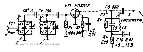
Fig. 8. Radio frequency amplifier.
A loop in the drain circuit can also be used to gain additional selectivity by eliminating the shunt resistor and connecting the drain of the transistor to the tap of the loop coil to reduce the gain.
A diagram of such an RF amplifier for a range of 10 m is shown in Fig. 9. It provides a receiver sensitivity better than 0.25 μV. In the amplifier, you can use two-gate transistors KP306, KP350 and KP326, which have a low throughput capacity, which contributes to the stability of the RF amplifier with a resonant load.

Fig. 9. URCH on a two-gate transistor.
The transistor mode is set by selecting resistors R1 and R3 so that the current consumed from the power source is 4 ... 7 mA. The gain is selected by moving the tap of the L3 coil and, when the coil is fully turned on, reaches 20 dB.
Loop coils L2 and L3 are wound on K10X6X4 rings made of 30VCh ferrite and have 16 turns of PELSHO 0.25 wire. Communication coils with antenna and mixer contain 3-5 turns of the same wire. It is easy to enter the AGC signal into the amplifier by feeding it to the second gate of the transistor. When the potential of the second gate drops to zero, the gain decreases by 40 ... 50 dB.
Literature: V.T. Polyakov. To radio amateurs about the direct conversion technique. M. 1990
High frequency amplifiers (UHF) are used to increase the sensitivity of radio receivers - radios, televisions, radio transmitters. Placed between the receiving antenna and the input of a radio or television receiver, such UHF circuits increase the signal coming from the antenna (antenna amplifiers).
The use of such amplifiers makes it possible to increase the radius of reliable radio reception, in the case of radio stations (transceiver devices - transceivers), either increase the operating range, or while maintaining the same range, reduce the radiation power of the radio transmitter.
Figure 1 shows examples of UHF circuits often used to increase the sensitivity of radio equipment. The values \u200b\u200bof the elements used depend on specific conditions: on the frequencies (lower and upper) of the radio range, from the antenna, from the parameters of the subsequent cascade, from the supply voltage, etc.
Figure 1 (a) shows broadband UHF circuit according to the scheme with a common emitter (OE). Depending on the transistor used, this circuit can be successfully applied up to frequencies of hundreds of megahertz.
It should be recalled that the reference data for transistors gives the limiting frequency parameters. It is known that when assessing the frequency capabilities of a transistor for a generator, it is enough to focus on the limiting value of the operating frequency, which should be at least two to three times lower than the limiting frequency specified in the passport. However, for an HF amplifier connected according to the OE scheme, the limiting passport frequency must already be reduced by at least an order of magnitude or more.
Fig. 1. Examples of circuits of simple high frequency amplifiers (UHF) on transistors.
Radioelements for the circuit in Fig. 1 (a):
- R1 \u003d 51k (for silicon transistors), R2 \u003d 470, R3 \u003d 100, R4 \u003d 30-100;
- C1 \u003d 10-20, C2 \u003d 10-50, C3 \u003d 10-20, C4 \u003d 500-Zn;
Capacitor values \u200b\u200bare for VHF frequencies. Capacitors such as KLS, KM, KD, etc.
Transistor stages, as you know, connected according to the common emitter (OE) scheme, provide a relatively high gain, but their frequency properties are relatively low.
Transistor stages, connected according to a common base (OB) circuit, have less gain than transistor circuits with an OE, but their frequency properties are better. This allows the use of the same transistors as in OE circuits, but at higher frequencies.
Figure 1 (b) shows high frequency broadband amplifier (UHF) circuit on one transistor turned on according to the scheme with a common base... An LC circuit is included in the collector circuit (load). Depending on the transistor used, this circuit can be successfully applied up to frequencies of hundreds of megahertz.
Radioelements for the circuit in Fig. 1 (b):
- R1 \u003d 1k, R2 \u003d 10k. R3 \u003d 15k, R4 \u003d 51 (for ZV-5V supply voltage). R4 \u003d 500-3 k (for supply voltage 6V-15V);
- C1 \u003d 10-20, C2 \u003d 10-20, C3 \u003d 1n, C4 \u003d 1n-3n;
- T1 - silicon or germanium RF transistors, for example. KT315. KT3102, KT368, KT325, GT311, etc.
Capacitor and loop values \u200b\u200bare for VHF frequencies. Capacitors such as KLS, KM, KD, etc.
Coil L1 contains 6-8 turns of PEV 0.51 wire, brass cores 8 mm long with M3 thread, a branch from 1/3 of the turns.
Figure 1 (c) shows another scheme of a broadband UHF on one transistorincluded according to the scheme with a common base... An RF choke is included in the collector circuit. Depending on the transistor used, this circuit can be successfully applied up to frequencies of hundreds of megahertz.
Radioelements:
- R1 \u003d 1k, R2 \u003d 33k, R3 \u003d 20k, R4 \u003d 2k (for 6V supply voltage);
- C1 \u003d 1n, C2 \u003d 1n, C3 \u003d 10n, C4 \u003d 10n-33n;
- T1 - silicon or germanium HF transistors, for example, KT315, KT3102, KT368, KT325, GT311, etc.
The values \u200b\u200bof the capacitors and the circuit are given for the frequencies of the MF-, HF-range. For higher frequencies, for example, for the VHF range, the capacitance values \u200b\u200bshould be reduced. In this case, chokes D01 can be used.
Capacitors such as KLS, KM, KD, etc.
L1 coils are chokes, for the CB range these can be coils on rings 600NN-8-K7x4x2, 300 turns of wire PEL 0.1.
Greater gain value can be obtained by applying multi-transistor circuits... These can be various circuits, for example, based on the OK-OB cascode amplifier on transistors of different structures with series power supply. One of the variants of such a UHF scheme is shown in Fig. 1 (d).
This UHF circuit has significant amplification (tens and even hundreds of times), but cascode amplifiers cannot provide significant amplification at high frequencies. Such schemes, as a rule, are used at frequencies of the LW and MW ranges. However, with the use of ultra-high frequency transistors and careful execution, such circuits can be successfully applied up to frequencies of tens of megahertz.
Radioelements:
- R1 \u003d 33k, R2 \u003d 33k, R3 \u003d 39k, R4 \u003d 1k, R5 \u003d 91, R6 \u003d 2.2k;
- C1 \u003d 10n, C2 \u003d 100, C3 \u003d 10n, C4 \u003d 10n-33n. C5 \u003d 10n;
- T1 -GT311, KT315, KT3102, KT368, KT325, etc.
- T2 -GT313, KT361, KT3107, etc.
Capacitor and loop values \u200b\u200bare for CB frequencies. For higher frequencies, eg for the HF range, the capacitance and loop inductance (number of turns) must be reduced accordingly.
Capacitors such as KLS, KM, KD, etc. Coil L1 - for the CB range, contains 150 turns of PELSHO 0.1 wire on 7 mm frames, trimmers M600NN-3-SS2.8x12.
When setting up the circuit in Fig. 1 (d), it is necessary to select resistors R1, R3 so that the voltages between the emitters and collectors of the transistors become the same and amount to 3V at a circuit supply voltage of 9 V.
The use of transistor UHF allows amplifying radio signals. coming from antennas, in TV bands - meter and decimeter waves... In this case, the most often used are antenna amplifier circuits built on the basis of circuit 1 (a).
Antenna amplifier circuit example for the frequency range 150-210 MHz is shown in Fig. 2 (a).

Figure 2.2. Scheme of an antenna amplifier of the MV range.
Radioelements:
- R1 \u003d 47k, R2 \u003d 470, R3 \u003d 110, R4 \u003d 47k, R5 \u003d 470, R6 \u003d 110. R7 \u003d 47k, R8 \u003d 470, R9 \u003d 110, R10 \u003d 75;
- C1 \u003d 15, C2 \u003d 1n, C3 \u003d 15, C4 \u003d 22, C5 \u003d 15, C6 \u003d 22, C7 \u003d 15, C8 \u003d 22;
- T1, T2, TZ - 1T311 (D, L), GT311D, GT341 or similar.
Capacitors such as KM, KD, etc. The frequency band of this antenna amplifier can be expanded in the low frequency region by a corresponding increase in the capacitances that make up the circuit.
Radio elements for the version of the antenna amplifier for the range 50-210 MHz:
- R1 \u003d 47k, R2 \u003d 470, R3 \u003d 110, R4 \u003d 47k, R5 \u003d 470, R6 \u003d 110. R7 \u003d 47k, R8 \u003d 470. R9 \u003d 110, R10 \u003d 75;
- C 1 \u003d 47, C2 \u003d 1n, C3 \u003d 47, C4 \u003d 68, C5 \u003d 47, C6 \u003d 68, C7 \u003d 47, C8 \u003d 68;
- Т1, Т2, ТЗ - ГТ311А, ГТ341 or similar.
Capacitors such as KM, KD, etc. When repeating this device, all requirements must be observed. HF structures for installation: minimum lengths of connecting conductors, shielding, etc.
Antenna amplifier designed for use in the ranges of television signals (and higher frequencies) can be overloaded with signals from powerful CB, HF, VHF radio stations. Therefore, a wide frequency band may not be optimal because this can interfere with the normal operation of the amplifier. This is especially true in the lower area of \u200b\u200bthe amplifier operating range.
For the circuit of the given antenna amplifier, this can be significant, since the slope of the gain rolloff at the lower end of the range is relatively low.
To increase the slope of the frequency response (AFC) of this antenna amplifier, you can use 3rd order high pass filter... For this, an additional LC circuit can be used at the input of the specified amplifier.
The connection diagram of the additional LC high-pass filter to the antenna amplifier is shown in Fig. 2 (b).
Additional filter parameters (approximate):
- C \u003d 5-10;
- L - 3-5 turns of PEV-2 0.6. winding diameter 4 mm.
It is advisable to adjust the frequency band and shape of the frequency response using appropriate measuring instruments (oscillator, etc.). The shape of the frequency response can be adjusted by changing the values \u200b\u200bof the capacitors C, C1, changing the pitch between the turns of L1 and the number of turns.
Using the described circuitry solutions and modern high-frequency transistors (microwave transistors - microwave transistors), you can build an antenna amplifier for the UHF range.This amplifier can be used both with a UHF radio receiver, for example, that is part of a VHF radio station, or together with a TV.
Figure 3 shows uHF antenna amplifier circuit.

Fig. 3. UHF range antenna amplifier diagram and connection diagram.
The main parameters of the UHF amplifier range:
- Frequency band 470-790 MHz,
- Gain - 30 dB,
- Noise figure -3 dB,
- Input and output resistance - 75 Ohm,
- Consumption current - 12 mA.
One of the features of this circuit is the supply voltage to the antenna amplifier circuit through the output cable, through which the output signal from the antenna amplifier is supplied to the radio signal receiver - a VHF radio receiver, for example, a VHF radio station or TV receiver.
Antenna amplifier consists of two transistor stages connected in a common emitter circuit. A high-pass filter of the 3rd order is provided at the input of the antenna amplifier, limiting the operating frequency range from below. This increases the noise immunity of the antenna amplifier.
Radioelements:
- R1 \u003d 150k, R2 \u003d 1k, R3 \u003d 75k, R4 \u003d 680;
- C1 \u003d 3.3, C10 \u003d 10, C3 \u003d 100, C4 \u003d 6800, C5 \u003d 100;
- T1, T2 - KT3101A-2, KT3115A-2, KT3132A-2.
- Capacitors C1, C2 type KD-1, the rest - KM-5 or K10-17v.
- L1 - PEV-2 0.8 mm, 2.5 turns, winding diameter 4 mm.
- L2 - RF choke, 25 μH.
Figure 3 (b) shows a diagram of connecting an antenna amplifier to the antenna jack of a TV receiver (to the UHF range selector) and to a remote 12V power source. In this case, as can be seen from the diagram, power is supplied to the circuit through a coaxial cable used and for transmitting the amplified UHF radio signal from the antenna amplifier to a receiver - a VHF radio receiver or to a TV.
Radio elements of connection, Fig. 3 (b):
- C5 \u003d 100;
- L3 - HF choke, 100 μH.
Installation is made on double-sided fiberglass SF-2 in a hinged way, the length of the conductors and the area of \u200b\u200bthe contact pads are minimal, it is necessary to provide for careful shielding of the device.
Setting up the amplifier is reduced to setting the collector currents of the transistors and are regulated using R1 and RЗ, T1 - 3.5 mA, T2 - 8 mA; the shape of the frequency response can be adjusted by selecting C2 in the range of 3-10 pF and changing the pitch between the turns of L1.
Literature: Rudomedov E.A., Rudometov V.E. - Electronics and espionage passions-3.
Panasyuk Anatoly Georgieaich
Position: teacher
Educational institution: GBPOU KK "Krasnodar College of Electronic Instrumentation"
Locality: Krasnodar
Material name: Radio receiving devices
Subject: RF Amplifiers
Date of publication: 05.01.2018
Section: secondary vocational
Amplifiers of a radio path
Chapter 3
Amplifiers of a radio path
3.1 Radio frequency amplifiers (RF amplifier), functions, basic
qualitative indicators.
3.1.1 RF amplifier circuits, RF amplifier stability.
The main functions of the RF amplifier.
1. Amplification of received signals at the carrier frequency required for
improving the real sensitivity of the RPRU.
2. Ensuring selectivity (selectivity) of RPRD to strong interference,
and selectivity for side reception channels (mirror channel, direct and
intermediate channel).
Key quality indicators.
1. Voltage gain
Ku \u003d Uoutx / Uin; K \u003d 20 lgKu
For a multi-stage RF amplifier, the overall gain is
K1xK2… ..Kn
2. Selectivity - shows how much the coefficient decreases
gain at the frequency of the interfering signal
Se \u003d Ko / K; Se \u003d\u003d 20lg Co / C
3. The bandwidth characterizes the bandwidth of the RF amplifier.
4. Range overlap ratio (span width)
5. Stability of work - characterizes the ability of the RF amplifier to maintain
main indicators when changing external and internal environmental factors
(temperature, supply voltage change).
Figure: 3.1 Generalized RF amplifier circuit
3.1.2 Analysis of the generalized circuit of a resonant single-circuit RF amplifier.
The input of the UE (amplifying device) receives a signal that is necessary
weekend
electrode
oscillatory circuit (Lk, Ck). The output signal is removed from the loop and
is fed to the input of the next stage, the conductivity of which is Y
in general, the oscillatory circuit is connected to the output electrode of the UP
and partial load, with inclusion factors ml and m2. coefficient
inclusion is called the ratio of the part of the voltage removed from the circuit
(Uout) to the total voltage on the circuit (U
In the general case, the resonant gain is
where ml m2 is the inclusion coefficient
S is the slope of the amplifier characteristics
Resonant loop impedance
3.1.3 Schematic diagram of the RF amplifier with autotransformer switching
circuit and autotransformer connection with the next cascade.
Figure: 3.2 Schematic diagram of the RF amplifier
Amplifiers of a radio path
admission
stresses
frequency
resonant
collector
transistor
alternating current l appears
Flowing through the resonant circuit (Lk, Ck, Cn)
the alternating component of the collector current creates a drop on it
voltage Un. Part of this voltage is removed from the tap of the loop coil
Lk, and is fed through the coupling capacitor Sat to the next stage (base
transistor UT2). The base of the bipolar transistor VT2 is connected to the part
output resonant circuit Lk Sk, in order to avoid its strong shunting
small (1500 - 2500 ohms) input resistance of the transistor. Coefficient
inclusion m2, characterizing the degree of connection between the base of the transistor VT2 with
resonant circuit Lc CK is always much less than unity. Collector
transistor VT1 is connected to part of the circuit. Incomplete connection of the collector with
circuit Lk, Sk, Sp is used to weaken the bypass circuit
the output circuit of the transistor and to ensure the stable operation of the cascade.
3.1.4 RP stability.
Under certain conditions, the reactor plant can self-excite and work as
an oscillator with a frequency close to its resonant frequency. This is due to the presence
internal feedback through a transistor (intra-transistor capacitive
OS due to the capacity of the collector-base transition).
When creating an amplifier, it is important that it not only does not self-excite,
but even with the necessary margin, stability was ensured when exposed to
various
destabilizing
factors
climatic mechanical influences, heating of the UE) such a margin is achieved
when the condition is met:
where: Ko is the resonant gain determined from the formula
above; Bush is a stable gain of the stage.
where: S - transistor slope
Ck - internal transistor capacitance of the OS, equal to the capacitance of the collector junction
3.1.5 Measures to increase the RP stability.
1.For an RF amplifier with a fixed setting to boost
stability, the neutralization of the capacity Sk is applied.
RF amplifier circuit with neutralization
Figure: 3.3 Amplifier circuit with neutrolization
actions
consists
administered
additional
an electrical circuit that is opposite in its properties
conductivity of the OS. The introduction of a sequential chain of Rn and Cn should be
such that the phase of the neutralization voltage is rotated by
180 ° relative to the feedback voltage. Often used to neutralize
only one container.
2. URCH with a transistor connected according to the scheme with OB.
In such RF amplifier, the base area of \u200b\u200bthe transistor when connected to a common point
the circuit drastically weakens the capacitive coupling between the input and output of the amplifier,
thereby increasing its stability.
Figure: 3.4 URCH circuit with OB
Amplifiers of a radio path
sustainability
transistor
operable in a wider frequency band. The connection of the transistor with
output circuit autotransformer, with input circuit through
capacitive
divider,
input
source
transformer,
weekend
subsequent
cascade
autotransformer. The RF amplifier is used in VHF receivers.
4. Cascade RF amplifier. Such a scheme is called a scheme in which
two different schemes for switching on amplifying devices are used.
The most common combination of OE - OB switching circuits.
Figure: 3.5 Cascode RF amplifier
Cascode circuits combine the high amplification properties of a circuit
inclusion
significant
weekend
resistance
stability of the circuit with OB .. Cascade amplifiers provide more
higher stable gain than a two stage amplifier on the same
transistors.
Transistor VT1 of the first stage of the cascade amplifier is switched on according to the scheme
provides
enough
resistance
amplifier; the selectivity (selectivity) of the signal source circuit
decreases slightly. The VT1 collector circuit is loaded with a small
input impedance of the second stage of the cascade amplifier included
according to the scheme with OB. For this reason, the first amplifier stage provides
signal amplification is practically only in power, and the second in voltage;
in general, the amplifier provides high gain in both power and
stress. It is used in VHF radio transmitters.
3.2 Bandpass amplifiers.
Bandpass amplifiers are amplifiers whose frequency response is close to
rectangular.
Due to
strip
amplifiers
provide
uniform
gain
transmission
weakening
located
resonant
interfering
signals.
apply
quality
amplifiers
intermediate
frequency (UHF) РПрУ, providing a weakening of the influence of closely located
interfering
signals
neighboring
Stripe
amplifiers
in most cases, do not rebuild, i.e. designed to work
at one tuning frequency.
Figure: 3.6 Frequency response of the Band-pass amplifier
The best shape of the frequency response of the PU is achieved through the use of double-circuit
(multi-circuit)
resonant
special
fSS filters. They are electoral systems with high
slope, transmission ratio outside the bandwidth.
practice
apply
various
multi-circuit and multi-link, electromechanical, piezoelectric,
piezomechanical, piezoceramic.
3.2.1 Scheme of the IF amplifier on doubly connected circuits.
Figure: 3.7 RF amplifier circuit with DFT
Amplifiers of a radio path
Figure: 3.8 Achh URCH with DFT
With a critical connection between the circuits when B \u003d l, the frequency response has one
maximum, flattened top and good uniformity in the strip pr
sinking at B\u003e 1, the frequency response is obtained with two side maxima. When
increasing
increases
transmission
expands and at the same time increases the unevenness in the strip
transmission. At B< 1 АЧХ имеет один максимум но полоса пропускания
less than at B \u003d 1. Thus, the most advantageous connection between
contours is critical B \u003d 1.
strip
amplifier
comparison
single-circuit RU is distinguished by a more rectangular shape, which indicates
better selectivity of a given frequency band.
3.2.2 IFA with a concentrated selection filter.
Figure 3.9 Scheme of RF amplifier with FSS on LC-links
discrete
elements
elements
oscillatory circuits, the connection between which is mainly capacitive, but
can be inductive and combined. The given scheme of the UPCH with FSS
double-circuit
agreed
wave
resistance
capacitive
contours.
transistor
autotransformer
subsequent
cascade
transformer. The degree of connection with the FSS is selected based on the agreement
output resistance VT1 and input resistance of the subsequent
cascade. To weaken the magnetic bonds between the coils, they are usually
placed on the screen. The outer contours L 1 С 1 and L3 C3 are half-links
FSS. The number of links in the FSS is determined by the number of capacitors
3.2.3 IF amplifier with Piezoceramic filter
dimensions,
manufacturing,
possess
attenuation in the passband and high squareness factor
transmission, which requires the inclusion of a resonant circuit before the filter
ensuring the matching of the output resistance of the transistor with
input resistance of the filter.
Figure: 3.10 UPCH with PCF
As an example, we give the data of a piezoceramic filter of the type
F P1P - 23 to an intermediate frequency of 465 kHz. Bandwidth per
level 0.5 (vdb) - 9.5 kHz, detuning selectivity: ± 9 kHz - 40 dB;
insertion loss in the passband no more than 9.5 dB Rin \u003d Kout \u003d 2 kOhm.
1. In UHF (UHF) receivers, single-loop are most widely used
transistor
amplifiers.
sustainable
gain
provide
cascading RF amplifier.
2. In the IF amplifier with distributed selection, most of the cascades are resonant
Amplifiers of a radio path
the resulting
determined
work
separate cascades. In the UPCH with concentrated selection, the resulting
The frequency response is mainly determined by the frequency response of the FSS, which is the load of one of
cascades of the IF amplifier (mixer), the rest of the cascades can be aperiodic or
broadband.
3. Filters on discrete LC are used as FSS in UPCH
Links, electromechanical, quartz and piezoceramic.
3.3 Amplifier circuits, designs and characteristics
radio signals
At moderately high frequencies, use the RF amplifier on bipolar (BT) and
field-effect (FET) transistors with high cutoff frequencies. Modern
integral
technology
allows
to manufacture
semiconductor
hybrid integrated circuits (ICs) of radio signal amplifiers (URCH)
and UCH) with external selective circuits (oscillatory circuits and
filters). It is also possible to use integral active RС-
filters, but their frequency properties are limited. Therefore, sometimes active
RC devices are used simultaneously with filter systems with
lumped parameters (contours, piezoceramic and other
filters). In this case, they act as amplifiers and devices
Figure: 3.11 RF amplifier circuits using a field-effect transistor IC
coordination.
given
transistor
transformer
including
vibrational
The oscillatory circuit is rebuilt by the varicap, to which the
control bias voltage Uу. Required cascade stability
achieved
coefficient
gain,
less
steady gain.
In fig. 3.11b, and a schematic diagram of an IC designed for
RF amplifier operating at frequencies up to 150 MHz, in Fig. 3.11, b - a variant of it
application. The circuit contains a cascode amplifier (OE-OB) on transistors
VT2 and VT1 for high stability. Using a transistor
VT3 regulates the gain of the IC, for which it is necessary
change the control voltage Uy at pin 9, which leads to
change
emitter
magnitudes
stresses
hence the emitter bias VT2. With diodes VD1, VD2,
resistors R1-R3 (temperature-dependent base bias divider) and
of feedback circuits, high stability of IC parameters is achieved:
temperature range from -60 to + 70 ° C change in Y 21 | does not exceed ± 25
%. The gain of the IC at a frequency of 10 MHz is not less than 200 (load resistance
100 Ohm), supply voltage 6.3 V (± 10%), power consumption 20 mW.
The IC is characterized by a relatively low noise level: at a frequency of 180 MHz
noise figure no more than 7 dB.
given
resonant
applied at frequencies up to 60 MHz. It contains IMS 175UV4, the base
which is a cascode amplifier with a differential stage.
The input signal from the circuit of the input circuit is fed to the base of the transistor VT4,
included in the circuit with the OE, and is further amplified by the transistor VT3 (OB)
This inclusion allows you to increase the stability of the amplifier and increase
Figure: 3.12 Schematic diagram of the RF amplifier on the IC 175UV4 working in
frequency range
Amplifiers of a radio path
its output impedance, which allows full switching on of the load
Adjustment
amplification
carried out
control voltage: Uy to the base of the differential transistor VT2
cascade. Since the emitter current of the transistor VT3 remains constant, then
the input impedance of the RF amplifier does not change during the gain adjustment,
which stabilizes the frequency response of the amplifier in a wide range of its
gain.
output
rebuild
varicaps included in the varicap matrix. To reduce the influence
nonlinear effects in each of the circuits use two varicaps,
connected in series on alternating current, which allows to reduce
influence of nonlinearities of even orders.
At microwave frequencies, RF amplifiers are used on microwave transistors (up to centimeter
waves inclusive), microwave vacuum tubes (meter and decimeter
ranges), TWT, devices with "negative" resistance, and
parametric and quantum amplifiers.
Transistor amplifiers have recently become widespread in
Microwave technology. Along with BT, PTs with a Schottky barrier type shutter are used
(PTSh) based on gallium arsenide. In the latter case, you can increase
the operating frequency of the RF amplifier is up to 80 GHz (compared to 15 GHz for BT), which
is explained by the high mobility of carriers in the PTSh. At frequencies 0.3-30 GHz
the gain of transistor single-stage amplifiers is
about 5-6 dB at 3-4% of carrier bandwidth, noise figure about 6 dB
It is characteristic that the noise and power matching modes of the RF amplifier for PTSh
differ to a lesser extent than for BT. Structurally transistors
are made on the basis of a leadless crystal, a crystal with leads, in
Figure: 3.13 Microwave amplifier circuits
conditionally tight (not for all external influences) and completely
sealed structures.
As matching circuits at the input and output of the cascade use
transforming filters, made on segments of long lines, in
including strip, waveguides or lumped elements (in
long-wave part of the range). If the agreement is carried out in
wide frequency range, then the drop in the gain of the stage with
increasing frequency. Therefore, it is possible to carry out matching on the upper
range boundary, and at lower frequencies go to mismatch
to apply
frequency-dependent
devices
the elements
dissipative losses, which increase with increasing frequency. IN
as a result, it is possible to equalize the frequency response Kp and obtain a small
VSWR in a wide frequency range. The greatest application at microwave frequencies is
switching circuit with OE (OI), which allows you to get the greatest gain and
the best noise characteristics.
In fig. 3.13, and the electrical circuit of the low-noise amplifier is shown
range
centimeter
Structurally
performed
sapphire substrate on which thin-film resistors are applied,
inductors, capacitors and connecting elements. Conforming
transforming chains have the form of segments of strip lines (in Fig. 4.50
shaded). The amplifier parameters are as follows: Cr. \u003d 25 dB, range
amplified frequencies 3.5-4.2 GHz, Ksh \u003d 5 dB, VSWR< 2, потребляемый ток 30
mA at 12V source voltage.
Balanced amplifiers are also used at microwave frequencies, block diagram
which is shown in Fig. 3.13, b As you can see, the input signal power through
the directional divider goes to two identical amplifying stages,
and then summed in a directional adder. Resistors Rbal. are
absorbing, which improves matching and provides a low VSWR at
Amplifiers of a radio path
QUESTIONS FOR SELF-CONTROL AND REPEAT
demands
are presented
amplifiers
radio signals
dependence on their area of \u200b\u200bapplication?
2. Name and compare the different types of parameters used to
descriptions of amplifying devices in the amplifier of radio signals.
3. What is the essence of the immitant research method
stability of the radio amplifier?
4. What is the difference between the gain stability factor and the gain?
limiting amplification of the amplifier of radio signals?
5. Indicate the methods of combating generation in the amplifier of radio signals. In what
6. How to increase the gain of the amplifier of radio signals?
7. Draw a diagram of resonant RF amplifier, indicate the purpose of all elements.
8. How does the resonant gain change over the frequency range?
URCH? How to eliminate the influence of unevenness of its characteristics on work
9. What are the advantages of a cascode RF amplifier?
Draw
strip
amplifiers
radio frequencies,
assignment of all elements.
11. What are the dependences of the main characteristics of a band-pass amplifier
high frequency from the number of stages?
12. Why is it possible to suppress reception interference in active filters without
using inductive components?
13. What are the features of the RC filters at high frequencies?
14. Compare the different types of high bandpass amplifiers
frequencies with highly efficient selective circuits.
characteristics
appliances
"negative" resistance?
16. Compare the features of the RF amplifier of different wavebands.
amplifier.
quality
divider
adder
use various devices, such as loop bridges (Fig. 3.14)
balance
amplifier
characteristically
gain,
difference
harmonization
power
dynamic range, but its use requires taking measures to
ensuring the identity of the arms of the amplifier.