We have a factory prototype board of this type at our disposal:
I don't like her for two reasons:
1) When installing parts, you have to constantly turn back and forth in order to first install the radio component, and then solder the conductor. It behaves unsteadily on the table.
2) After dismantling, the holes remain filled with solder; before the next use of the board, you have to clean them.
Having searched on the Internet for various types of breadboards that you can make with your own hands and from available materials, came across a few interesting options, one of which decided to repeat.
Option #1
Quote from the forum: « For example, I have been using these homemade ones for many years development boards. Assembled from a piece of fiberglass into which copper pins are riveted. Such pins can either be bought on the radio market or made yourself from copper wire with a diameter of 1.2-1.3 mm. Thinner pins bend too much, and thicker pins take up too much heat when soldering. This “breadboard” allows you to reuse the most shabby radioelements. It is better to make connections with wire in fluoroplastic insulation MGTF. Then, once made, the ends will last a lifetime.”
I think this option will suit me best. But fiberglass and ready-made copper pins are not available, so I’ll do it a little differently.
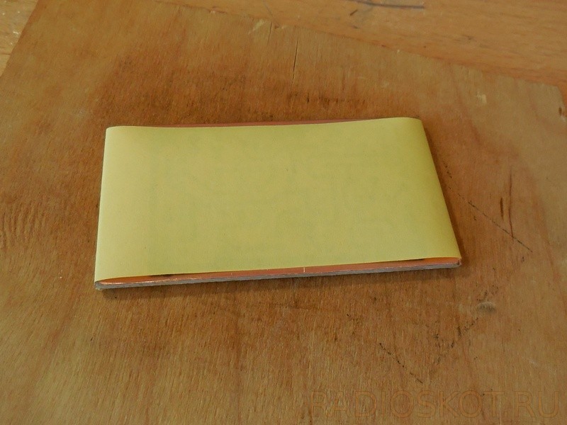
Copper wire extracted from the wire:

I stripped the insulation and, using a simple limiter, made pins of the same length:

Pin diameter - 1 mm.

I used thick plywood as the basis for the board. 4 mm (The thicker it is, the stronger the pins will hold.):

In order not to have to worry about markings, I taped the lined paper onto the plywood:

And drilled holes in increments 10 mm drill diameter 0.9 mm:

We get even rows of holes:

Now you need to drive the pins into the holes. Since the diameter of the hole is smaller than the diameter of the pin, the connection will be tight and the pin will be tightly fixed in the plywood.

When driving pins under the bottom of the plywood, you need to place a metal sheet. The pins are driven in with light movements, and when the sound changes, it means the pin has reached the sheet.
To prevent the board from fidgeting, we make legs:

Glue:

The breadboard is ready!
Using the same method, you can make a surface-mount board (photo from the Internet, radio):

Below, to complete the picture, I will present several suitable designs found on the Internet.
Option No. 2Push pins with a metal head are hammered into a section of the board:

All that remains is to tin them. Copper-plated buttons can be tinned without problems, but with steel ones. 
Let's look at the process of making printed circuit boards at home at specific example. You need to make two boards. One is an adapter from one type of case to another. The second is replacing a large microcircuit with a BGA package with two smaller ones, with TO-252 packages, with three resistors. Board sizes: 10x10 and 15x15 mm. There are several options for making printed circuit boards at home. The most popular ones are using photoresist and “iron-laser technology”.
Instructions for making printed circuit boards at home
You will need
- personal computer with a program for tracing printed circuit boards;
- laser printer;
- thick paper;
- fiberglass;
- iron;
- hacksaw;
- acid for etching the board.
1 Project preparation printed circuit board
We are preparing a printed circuit board project. I use the DipTrace program: convenient, fast, high quality. Developed by our compatriots. Very convenient and pleasant user interface, unlike the generally accepted PCAD. Free for small projects. Libraries of electronic components housings, including 3D models. There is a conversion to PCAD PCB format. Many domestic firms have already begun to accept projects in the DipTrace format.
PCB design
The DipTrace program allows you to see your future creation in volume, which is convenient and visual. This is what I should get (the boards are shown in different scales):

2 Marking fiberglass laminate
First, we mark the PCB and cut out the blank for the printed circuit boards.

3 Project output on a laser printer
We output the project on a laser printer in a mirror image to the maximum possible quality, without skimping on toner. After much experimentation, I was chosen best paper For this purpose - thick matte paper for printers. You can try using photo paper or buy special thermal paper.

4 Transferring a project for fiberglass
Let's clean and degrease the board blank. If you don’t have a degreaser, you can go over the copper foil of fiberglass with a regular eraser. Next, using an iron, we “weld” the toner from the paper to the future printed circuit board. I hold it for 3-4 minutes under slight pressure until the paper turns slightly yellow. I set the heat to maximum. I put another sheet of paper on top for more even heating, otherwise the image may “float”.
The important point here is the uniformity of heating and pressure and heating time. If you don't hold the iron down enough, the print will be washed away during etching, and the tracks will be corroded by acid. If you overexpose it, nearby conductors may merge with each other.

5 Removing the paper from the workpiece
After this, we place the workpiece with the paper stuck to it in the water. You don’t have to wait for the textolite to cool down. Photo paper quickly gets wet, and after a minute or two you can carefully remove the top layer.

In places where there is a large concentration of our future conductive paths, the paper sticks to the board especially strongly. We're not touching it yet. Let the board soak for a couple more minutes. Now the remaining paper is removed using an eraser or rubbing with your finger. You should end up with a beautiful, clean piece with a clearly printed design.
 Removing the remaining paper from the printed circuit board blank
 6 Preparing the board for etching
We take out the workpiece. Dry it. If somewhere the tracks are not very clear, you can make them brighter with a thin CD marker or nail polish, for example (depending on what you are going to etch the board with).

It is necessary to ensure that all the paths come out clear, even and bright. It depends on the:
- uniformity and sufficiency of heating the workpiece with an iron;
- be careful when removing paper;
- quality of PCB surface preparation;
- good selection of paper.
Experiment with different types paper, different heating times, different types of fiberglass surface cleaning to find the most optimal quality option. By choosing an acceptable combination of these conditions, in the future you will be able to produce printed circuit boards at home faster and with better quality.
7 Etching printed circuit board
We place the resulting workpiece with future conductor tracks printed on it in an acid, for example, in a solution of ferric chloride. We'll talk about other types of etching later. We poison for 1.5 or 2 hours. While we wait, cover the bath with a lid: the fumes are quite caustic and toxic.

8 Flushing printed circuit board
We take the finished boards out of the solution, wash and dry. Toner from a laser printer can be easily washed off the board using acetone. As you can see, even the thinnest conductors with a width of more than 0.2 mm came out quite well. There is very little left.

8 Tinning printed circuit board
We tin the manufactured printed circuit boards. We wash off the remaining flux with gasoline or an alcohol-gasoline mixture.
All that remains is to cut out the boards and mount the radio elements!
conclusions
With some skill, the “laser-iron method” is suitable for making simple printed circuit boards at home. Conductors from 0.2 mm and thicker are clearly obtained. Time for preparation, experiments with selecting the type of paper and iron temperature, etching and tinning takes approximately 2 to 5 hours. When you find the optimal combination, the time spent on making the board will be less than 2 hours. This is much faster than ordering boards from a company. Cash costs are also minimal. In general, for simple budget amateur radio projects, the method is recommended for use.
Recently, radio electronics as a hobby in the world is gaining popularity, people are becoming interested with my own hands create electronic devices. There are a huge number of circuits on the Internet, from simple to complex, performing various tasks, so everyone can find something they like in the world of radio electronics.
An integral part of any electronic device is a printed circuit board. It is a plate of dielectric material on which copper conductive tracks are applied connecting electronic components. Each of those who want to learn how to assemble electrical circuits in a beautiful form must learn how to make these same printed circuit boards.
Exist computer programs, which allow you to draw a pattern of PCB tracks in a convenient interface, the most popular of them is. The layout of the printed circuit board is carried out in accordance with circuit diagram devices, there is nothing complicated about it, you just need to connect the tracks necessary details. In addition, to many schemes electronic devices ready-made drawings of printed circuit boards are already attached on the Internet.
A good printed circuit board is the key to long and happy operation of the device, so you should try to make it as carefully and efficiently as possible. The most common method of making printed ones at home is the so-called “”, or “laser-ironing technology”. It has gained wide popularity because it does not take much time, does not require scarce ingredients, and is not so difficult to learn. Briefly, LUT can be described as follows: let's say there is a pattern of tracks drawn on a computer. Next, this drawing needs to be printed on special thermal transfer paper, transferred to textolite, then the excess copper should be etched from the board, holes drilled in in the right places and tin the paths. Let's look at the whole process step by step:
Printing a board design
1) Printing a design on thermal transfer paper. You can buy such paper, for example, on Aliexpress, where it costs mere pennies - 10 rubles per A4 sheet. Instead, you can use any other glossy paper, for example, from magazines. However, the quality of toner transfer from such paper may be much worse. Some people use Lomond glossy photo paper, a good option, if not for the price, such photo paper costs much more. I recommend trying to print the drawing on different papers, and then compare which one produces the best result.
Another important point when printing a picture - printer settings. It is imperative to disable toner saving, but the density should be set to maximum, because the thicker the toner layer, the better for our purposes.

You also need to take into account the fact that the design will be transferred to the textolite in a mirror image, so you need to foresee in advance whether or not you need to mirror the design before printing. This is especially critical on boards with microcircuits, because it will not be possible to install them on the other side.

Preparing PCB for transferring a drawing onto it
2) The second stage is preparing the textolite for transferring the drawing onto it. Most often, textolite is sold in pieces measuring 70x100 or 100x150 mm. You need to cut a piece that fits the dimensions of the board, with a margin of 3-5 mm at the edges. It is most convenient to saw PCB with a hacksaw or a jigsaw; in extreme cases, it can be cut off with metal scissors. Then, this piece of PCB should be wiped with fine sandpaper or a hard eraser. On the surface of the copper foil, small-minor scratches, This is fine. Even if the PCB initially looks perfectly smooth, this step is necessary, otherwise it will be difficult to tin it later. After sanding, the surface must be wiped with alcohol or solvent to wash off dust and greasy hand marks. After this, you cannot touch the copper surface.


Transferring the drawing to the prepared textolite
3) The third stage is the most critical. It is necessary to transfer the drawing printed on thermal transfer paper to the prepared textolite. To do this, cut the paper as shown in the photo, leaving some margin around the edges. On a flat wooden board we place the paper with the pattern facing up, then we apply textolite on top, copper to the paper. We bend the edges of the paper as if it were hugging a piece of PCB. After this, carefully turn the sandwich over so that the paper is on top. We check that the drawing has not shifted anywhere relative to the PCB and place a clean piece of ordinary office white paper on top so that it covers the entire sandwich.


Now all that remains is to heat the whole thing thoroughly, and all the toner from the paper will end up on the PCB. You need to apply a heated iron on top and heat the sandwich for 30-90 seconds. The heating time is selected experimentally and largely depends on the temperature of the iron. If the toner transfers poorly and remains on the paper, you need to keep it longer, but if, on the contrary, the tracks transfer, but are smeared, this is a clear sign of overheating. There is no need to put pressure on the iron; its own weight is enough. After warming up, you need to remove the iron and iron the still hot workpiece with a cotton swab, in case in some places the toner did not transfer well when ironing. After this, all that remains is to wait until the future board cools down and remove the thermal transfer paper. It may not work out the first time, it doesn’t matter, because experience comes with time.
PCB etching
4) The next stage is etching. Any area of copper foil that is not covered by toner should be removed, leaving the copper underneath the toner untouched. First you need to prepare a solution for etching copper, the simplest, most affordable and cheap option- a solution of citric acid, salt and hydrogen peroxide. In a plastic or glass container you need to mix one or two tablespoons of citric acid and a teaspoon of table salt per glass of water. Proportions do not play a big role, you can pour it by eye. Mix thoroughly and the solution is ready. You need to put the board in it, tracks down, to speed up the process. You can also slightly warm the solution, this will further increase the speed of the process. After about half an hour, all the excess copper will be etched away and only the tracks will remain.


Wash toner off tracks
5) The hardest part is over. At the fifth stage, when the board is already etched, you need to wash off the toner from the tracks with a solvent. Most affordable option- women's nail polish remover, it costs a penny and almost every woman has it. You can also use common solvents, such as acetone. I use petroleum solvent; although it stinks a lot, it doesn’t leave any black marks on the board. As a last resort, you can remove the toner by thoroughly rubbing the board with sandpaper.

Drilling holes on the board
6) Drilling holes. You will need a small drill with a diameter of 0.8 - 1 mm. Conventional high-speed steel drills quickly become dull on PCB, so it is best to use tungsten carbide drills, although they are more fragile. I drill boards using a motor from an old hair dryer with a small collet chuck, the holes are smooth and without burrs. Unfortunately, the last carbide drill bit broke at the most inopportune moment, so only half of the holes are drilled in the photos. The rest can be drilled later.


Tin the tracks
7) All that remains is to tin the copper tracks, i.e. cover with a layer of solder. Then they will not oxidize over time, and the board itself will become beautiful and shiny. First you need to apply flux to the tracks, and then quickly move a soldering iron with a drop of solder over them. You should not apply an excessively thick layer of solder, otherwise the holes may close and the board will look sloppy.

At this point, the manufacturing process of the printed circuit board is completed, and now you can solder parts into it. Material provided for the Radioschemes website by Mikhail Gretsky, [email protected]
Discuss the article MANUFACTURING PRINTED BOARDS WITH LUT
How to prepare a board made in Eagle for production
Preparation for production consists of 2 stages: technology constraint check (DRC) and generation of Gerber files
DRC
Each manufacturer of printed circuit boards has technological restrictions on the minimum width of tracks, gaps between tracks, hole diameters, etc. If the board does not meet these restrictions, the manufacturer refuses to accept the board for production.
When creating a PCB file, the default technology constraints are set from the default.dru file in the dru directory. Typically, these limits do not match those of real manufacturers, so they need to be changed. It is possible to set the restrictions just before generating the Gerber files, but it is better to do this immediately after generating the board file. To set restrictions, press the DRC button
Gaps
Go to the Clearance tab, where you set the gaps between the conductors. We see 2 sections: Different signals And Same signals. Different signals- determines the gaps between elements belonging to different signals. Same signals- determines the gaps between elements belonging to the same signal. As you move between input fields, the picture changes to show the meaning of the entered value. Dimensions can be specified in millimeters (mm) or thousandths of an inch (mil, 0.0254 mm).
![]()
Distances
On the Distance tab, the minimum distances between the copper and the edge of the board are determined ( Copper/Dimension) and between the edges of the holes ( Drill/Hole)
Minimum dimensions
On the Sizes tab for double-sided boards, 2 parameters make sense: Minimum Width- minimum conductor width and Minimum Drill- minimum hole diameter.
Belts
On the Restring tab, you set the sizes of the bands around vias and contact pads of lead components. The width of the belt is set as a percentage of the hole diameter, and you can set a limit on the minimum and maximum width. For double-sided boards the parameters make sense Pads/Top, Pads/Bottom(pads on the top and bottom layer) and Vias/Outer(vias).
Masks
On the Masks tab, you set the gaps from the edge of the pad to the solder mask ( Stop) and solder paste ( Cream). Clearances are set as a percentage of the smaller pad size, and you can set a limit on the minimum and maximum clearance. If the board manufacturer does not specify special requirements, you can leave the default values on this tab.
Parameter Limit defines the minimum diameter of the via that will not be covered by the mask. For example, if you specify 0.6mm, then vias with a diameter of 0.6mm or less will be covered by a mask.
Running a scan
After setting the restrictions, go to the tab File. You can save settings to a file by clicking the button Save As.... In the future, you can quickly download settings for other boards ( Load...).
At the touch of a button Apply established technology limitations apply to the PCB file. It affects layers tStop, bStop, tCream, bCream. Vias and pin pads will also be resized to meet the constraints specified in the tab Restring.
Button press Check starts the constraint monitoring process. If the board meets all restrictions, a message will appear in the program status line No errors. If the board does not pass inspection, a window appears DRC Errors

The window contains a list of DRC errors, indicating the error type and layer. When you double-click on a line, the area of the board with the error will be shown in the center of the main window. Error types:
gap too small
hole diameter too small
intersection of tracks with different signals
foil too close to the edge of the board
After correcting the errors, you need to run the control again and repeat this procedure until all errors are eliminated. The board is now ready to output to Gerber files.
Generating Gerber files
From the menu File choose CAM Processor. A window will appear CAM Processor.

The set of file generation parameters is called a task. The task consists of several sections. The section defines the output parameters of one file. By default, the Eagle distribution includes the task gerb274x.cam, but it has 2 drawbacks. Firstly, the lower layers are displayed in a mirror image, and secondly, the drilling file is not output (to generate the drilling, you will need to perform another task). Therefore, let's consider creating a task from scratch.
We need to create 7 files: board borders, copper on top and bottom, silkscreen on top, solder mask on top and bottom, and drill bit.
Let's start with the boundaries of the board. In field Section enter the section name. Checking what's in the group Style installed only pos. Coord, Optimize And Fill pads. From the list Device choose GERBER_RS274X. In the input field File The name of the output file is entered. It is convenient to place the files in a separate directory, so in this field we will enter %P/gerber/%N.Edge.grb . This means the directory where the board source file is located, the subdirectory gerber, original board file name (no extension .brd) with added at the end .Edge.grb. Please note that subdirectories are not created automatically, so you will need to create a subdirectory before generating files gerber in the project directory. In the fields Offset enter 0. In the list of layers, select only the layer Dimension. This completes the creation of the section.
To create a new section, click Add. A new tab appears in the window. We set the section parameters as described above, repeat the process for all sections. Of course, each section must have its own set of layers:
copper on top - Top, Pads, Vias
copper bottom - Bottom, Pads, Vias
silkscreen printing on top - tPlace, tDocu, tNames
mask on top - tStop
bottom mask - bStop
drilling - Drill, Holes
and the file name, for example:
copper on top - %P/gerber/%N.TopCopper.grb
copper bottom - %P/gerber/%N.BottomCopper.grb
silkscreen printing on top - %P/gerber/%N.TopSilk.grb
mask on top - %P/gerber/%N.TopMask.grb
bottom mask - %P/gerber/%N.BottomMask.grb
drilling - %P/gerber/%N.Drill.xln
For a drill file, the output device ( Device) should be EXCELLON, but not GERBER_RS274X
It should be kept in mind that some board manufacturers only accept files with names in 8.3 format, that is, no more than 8 characters in the file name, no more than 3 characters in the extension. This should be taken into account when specifying file names.
We get the following:

Then open the board file ( File => Open => Board). Make sure the board file has been saved! Click Process Job- and we get a set of files that can be sent to the board manufacturer. Please note that in addition to the actual Gerber files, information files will also be generated (with extensions .gpi or .dri) - you do not need to send them.

You can also display files only from individual sections by selecting the desired tab and clicking Process Section.
Before sending the files to the board manufacturer, it's helpful to preview what you've produced using a Gerber viewer. For example, ViewMate for Windows or for Linux. It can also be useful to save the board as a PDF (in the board editor File->Print->PDF button) and send this file to the manufacturer along with the gerberas. Because they are people too, this will help them not make mistakes.
Technological operations that must be performed when working with SPF-VShch photoresist
1. Surface preparation.
a) cleaning with polished powder (“Marshalit”), size M-40, washing with water
b) pickling with a 10% sulfuric acid solution (10-20 sec), rinsing with water
c) drying at T=80-90 gr.C.
d) check - if within 30 seconds. a continuous film remains on the surface - the substrate is ready for use,
if not, repeat all over again.
2. Application of photoresist.
Photoresist is applied using a laminator with Tshaft = 80 g.C. (see instructions for using the laminator).
For this purpose, the hot substrate (after drying cabinet) simultaneously with the film from the SPF roll is directed into the gap between the shafts, and the polyethylene (matte) film should be directed towards the copper side of the surface. After pressing the film to the substrate, the movement of the shafts begins, while the polyethylene film is removed, and the photoresist layer is rolled onto the substrate. The lavsan protective film remains on top. After this, the SPF film is cut on all sides to the size of the substrate and kept at room temperature within 30 minutes. Exposure for 30 minutes to 2 days in the dark at room temperature is allowed.
3. Exposure.
Exposure through a photomask is carried out on SKTSI or I-1 installations with UV lamps such as DRKT-3000 or LUF-30 with a vacuum vacuum of 0.7-0.9 kg/cm2. The exposure time (to obtain a picture) is regulated by the installation itself and is selected experimentally. The template must be pressed well to the substrate! After exposure, the workpiece is kept for 30 minutes (up to 2 hours is allowed).
4. Manifestation.
After exposure, the drawing is developed. For this purpose, the top protective layer, the lavsan film, is removed from the surface of the substrate. After this, the workpiece is dipped into a solution of soda ash (2%) at T = 35 g.C. After 10 seconds, begin the process of removing the unexposed part of the photoresist using a foam rubber swab. The time of manifestation is selected experimentally.
Then the substrate is removed from the developer, washed with water, and pickled (10 sec.) with a 10% solution of H2SO4 ( sulfuric acid), again with water and dried in a closet at T=60 deg.C.
The resulting pattern should not peel off.
5. The resulting drawing.
The resulting pattern (photoresist layer) is resistant to etching in:
- ferric chloride
- hydrochloric acid
- copper sulfate
- aqua regia (after additional tanning)
and other solutions
6. Shelf life of SPF-VShch photoresist.
The shelf life of SPF-VShch is 12 months. Storage is carried out in a dark place at a temperature of 5 to 25 degrees. C. in an upright position, wrapped in black paper.
Printed circuit board– this is a dielectric base, on the surface and in the volume of which conductive paths are applied in accordance with electrical diagram. The printed circuit board is designed for mechanical fastening and electrical connection between each other by soldering the leads of electronic and electrical products installed on it.
Operations for cutting out a workpiece from fiberglass, drilling holes and etching a printed circuit board to obtain current-carrying paths, regardless of the method of applying the pattern to printed circuit board are performed using the same technology.
Manual application technology
PCB tracks
Preparing the template
The paper on which the PCB layout is drawn is usually thin and for more accurate drilling of holes, especially when using manual homemade drill so that the drill does not lead to the side, it is necessary to make it more dense. To do this, you need to glue the printed circuit board design onto thicker paper or thin thick cardboard using any glue, such as PVA or Moment.

Cutting the workpiece
A blank of foil fiberglass laminate of a suitable size is selected, the printed circuit board template is applied to the blank and outlined around the perimeter with a marker, a soft pencil or marking with a sharp object.

Next, the fiberglass laminate is cut along the marked lines using metal scissors or sawed out with a hacksaw. Scissors cut faster and there is no dust. But we must take into account that when cutting with scissors, fiberglass is strongly bent, which somewhat worsens the adhesion strength of copper foil and if the elements need to be re-soldered, the tracks may peel off. Therefore, if the board is large and has very thin traces, then it is better to cut it using a hacksaw.

The template of the printed circuit board pattern is glued to the cut-out workpiece using Moment glue, four drops of which are applied to the corners of the workpiece.

Since the glue sets in just a few minutes, you can immediately begin drilling holes for radio components.
Drilling holes
It is best to drill holes using a special mini drilling machine with a carbide drill with a diameter of 0.7-0.8 mm. If mini drilling machine is not available, you can drill holes with a low-power drill using a simple drill. But when working universal hand drill The number of broken drills will depend on the hardness of your hand. You definitely won’t be able to get by with just one drill.

If you cannot clamp the drill, you can wrap its shank with several layers of paper or one layer of sandpaper. You can wrap a thin metal wire tightly around the shank, turn to turn.

After finishing drilling, check whether all holes are drilled. This can be clearly seen if you look at the printed circuit board up to the light. As you can see, there are no missing holes.
Applying a topographic drawing
In order to protect the places of foil on fiberglass laminate that will be conductive paths from destruction during etching, they must be covered with a mask that is resistant to dissolution in an aqueous solution. For the convenience of drawing paths, it is better to pre-mark them using a soft pencil or marker.
Before applying the markings, it is necessary to remove traces of the glue that was used to glue the printed circuit board template. Since the glue has not hardened much, it can be easily removed by rolling it with your finger. The surface of the foil must also be degreased using a rag using any means, for example acetone or white alcohol (the so-called purified gasoline), or any detergent for washing dishes, for example Ferry.

After marking the tracks of the printed circuit board, you can begin to apply their design. Any waterproof enamel is well suited for drawing paths, for example alkyd enamel PF series, diluted to a suitable consistency with white alcohol solvent. You can draw paths different instruments– a glass or metal drawing pen, a medical needle and even a toothpick. In this article I will tell you how to draw circuit board traces using a drawing pen and ballerina, which are designed for drawing on paper with ink.

Previously, there were no computers and all drawings were drawn with simple pencils on whatman paper and then transferred in ink to tracing paper, from which copies were made using copiers.
Drawing begins with contact pads, which are drawn with a ballerina. To do this, you need to adjust the gap of the sliding jaws of the ballerina drawing board to the required line width and to set the diameter of the circle, perform the adjustment with the second screw, moving the drawing blade away from the axis of rotation.
Next, the ballerina's drawing board is filled with paint to a length of 5-10 mm using a brush. For applying a protective layer to a printed circuit board, PF or GF paint is best suited, since it dries slowly and allows you to work quietly. NTs brand paint can also be used, but it is difficult to work with because it dries quickly. The paint should adhere well and not spread. Before painting, the paint must be diluted to a liquid consistency, adding a suitable solvent to it little by little with vigorous stirring and trying to paint on scraps of fiberglass. To work with paint, it is most convenient to pour it into a bottle of manicure varnish, in the twist of which there is a solvent-resistant brush installed.
After adjusting the ballerina's drawing board and obtaining the required line parameters, you can begin to apply the contact pads. To do this, the sharp part of the axis is inserted into the hole and the base of the ballerina is rotated in a circle.

With the correct setting of the drawing pen and the desired consistency of paint around the holes on the printed circuit board, perfect circles are obtained round shape. When a ballerina begins to paint poorly, the remaining dried paint is removed from the gap of the drawing board with a cloth and the drawing board is filled with fresh paint. To draw all the holes on this printed circuit board with circles it took only two refills of the drawing pen and no more than two minutes of time.
Once the round pads on the board are drawn, you can start drawing the conductive paths using a hand drawing pen. Preparing and adjusting a manual drawing board is no different from preparing a ballerina.
The only thing additionally needed is a flat ruler, with pieces of rubber 2.5-3 mm thick glued to one of its sides along the edges, so that the ruler does not slip during operation and the fiberglass, without touching the ruler, can freely pass under it. A wooden triangle is best suited as a ruler; it is stable and at the same time can serve as a hand support when drawing a printed circuit board.

To prevent the printed circuit board from slipping when drawing tracks, it is advisable to place it on a sheet of sandpaper, which consists of two sandpaper sheets sealed together with the paper sides.

If they come into contact when drawing paths and circles, then you should not take any measures. You need to let the paint on the printed circuit board dry until it does not stain when touched, and use the tip of a knife to remove the excess part of the design. In order for the paint to dry faster, the board should be placed in a warm place, for example, on a radiator in winter. IN summer time years - under the rays of the sun.

When the design on the printed circuit board is completely applied and all defects are corrected, you can proceed to etching it.
Printed circuit board design technology
using a laser printer
When printing on a laser printer, the image formed by the toner is transferred, due to electrostatics, from the photo drum on which the laser beam drew the image, onto paper. The toner is held onto the paper, preserving the image, only due to electrostatics. To fix the toner, the paper is rolled between rollers, one of which is a thermal oven heated to a temperature of 180-220°C. The toner melts and penetrates the paper texture. Once cooled, the toner hardens and adheres firmly to the paper. If the paper is heated again to 180-220°C, the toner will again become liquid. This property of toner is used to transfer images of current-carrying tracks onto a printed circuit board at home.
After the file with the printed circuit board design is ready, you need to print it using a laser printer onto paper. Please note that the image of the printed circuit board drawing for this technology must be viewed from the side where the parts are installed! Jet printer It is not suitable for these purposes, as it works on a different principle.
Preparing a paper template for transferring the design to the printed circuit board
If you print a printed circuit board design on ordinary paper for office equipment, then due to its porous structure, the toner will penetrate deeply into the body of the paper and when the toner is transferred to the printed circuit board, most of it will remain in the paper. In addition, there will be difficulties in removing paper from the printed circuit board. You will have to soak it in water for a long time. Therefore, to prepare a photomask, you need paper that does not have a porous structure, for example photo paper, a substrate from self-adhesive films and labels, tracing paper, pages from glossy magazines.
I use old stock tracing paper as the paper for printing the PCB design. Tracing paper is very thin and it is impossible to print a template directly on it; it gets wrinkled in the printer. To solve this problem, before printing, you need to apply a drop of any glue to a piece of tracing paper of the required size in the corners and glue it to a sheet of A4 office paper.

This technique allows you to print a printed circuit board design even on the thinnest paper or film. In order for the toner thickness of the drawing to be maximum, before printing, you need to configure the “Printer Properties” by turning off the economical printing mode, and if this function is not available, then select the coarsest type of paper, for example cardboard or something similar. It’s entirely possible that you won’t get a good print the first time, and you’ll have to experiment a little to find the best print mode for your laser printer. In the resulting print of the design, the tracks and contact pads of the printed circuit board must be dense without gaps or smudging, since retouching at this technological stage is useless.

All that remains is to cut the tracing paper along the contour and the template for making the printed circuit board will be ready and you can proceed to the next step, transferring the image onto fiberglass laminate.
Transferring a design from paper to fiberglass
Transferring the printed circuit board design is the most critical step. The essence of the technology is simple: paper, with the side of the printed pattern of the tracks of the printed circuit board, is applied to the copper foil of fiberglass and pressed with great force. Next, this sandwich is heated to a temperature of 180-220°C and then cooled to room temperature. The paper is torn off, and the design remains on the printed circuit board.
Some craftsmen suggest transferring a design from paper to a printed circuit board using an electric iron. I tried this method, but the result was unstable. It is difficult to simultaneously heat the toner to desired temperature and uniform pressing of the paper to the entire surface of the printed circuit board when the toner hardens. As a result, the pattern is not completely transferred and gaps remain in the pattern of the printed circuit board tracks. Perhaps the iron did not heat up enough, although the regulator was set to maximum heating iron. I didn’t want to open the iron and reconfigure the thermostat. Therefore, I used another technology, less labor-intensive and providing one hundred percent results.
On a piece of foil fiberglass laminate cut to the size of the printed circuit board and degreased with acetone, I glued tracing paper with a pattern printed on it in the corners. On top of the tracing paper I placed, for more even pressure, heels of sheets of office paper. The resulting package was placed on a sheet of plywood and covered on top with a sheet of the same size. This entire sandwich was clamped with maximum force in clamps.

All that remains is to heat the prepared sandwich to a temperature of 200°C and cool. An electric oven with a temperature controller is ideal for heating. It is enough to place the created structure in a cabinet, wait for the set temperature to reach, and after half an hour remove the board to cool.

If you don’t have an electric oven at your disposal, you can also use gas oven, adjusting the temperature using the gas supply knob using the built-in thermometer. If there is no thermometer or it is faulty, then women can help; the position of the control knob at which pies are baked is suitable.

Since the ends of the plywood were warped, I clamped them with additional clamps just in case. To avoid this phenomenon, it is better to clamp the printed circuit board between metal sheets 5-6 mm thick. You can drill holes in their corners and clamp printed circuit boards, tighten the plates using screws and nuts. M10 will be enough.
After half an hour, the structure has cooled enough for the toner to harden, and the board can be removed. At the first glance at the removed printed circuit board, it becomes clear that the toner transferred from tracing paper to the board perfectly. The tracing paper fits tightly and evenly along the lines printed tracks, pad rings and marking letters.

The tracing paper easily came off from almost all the traces of the printed circuit board; the remaining tracing paper was removed with a damp cloth. But still, there were gaps in several places on the printed tracks. This can happen as a result of uneven printing from the printer or remaining dirt or corrosion on the fiberglass foil. Gaps can be painted over with any waterproof paint, manicure polish, or retouched with a marker.

To check the suitability of a marker for retouching a printed circuit board, you need to draw lines on paper with it and moisten the paper with water. If the lines do not blur, then the retouching marker is suitable.

It is best to etch a printed circuit board at home in a solution of ferric chloride or hydrogen peroxide with citric acid. After etching, toner can be easily removed from the printed tracks with a swab soaked in acetone.
Then holes are drilled, conductive paths and contact pads are tinned, and radioelements are sealed.

This is the appearance of the printed circuit board with radio components installed on it. The result was a power supply and switching unit for electronic system, complementing an ordinary toilet with a bidet function.
PCB etching
To remove copper foil from unprotected areas of foiled fiberglass laminate when making printed circuit boards at home, radio amateurs usually use chemical method. The printed circuit board is placed in an etching solution and due to chemical reaction copper, unprotected by the mask, dissolves.
Recipes for pickling solutions
Depending on the availability of components, radio amateurs use one of the solutions given in the table below. Etching solutions are arranged in order of popularity of their use by radio amateurs at home.
| Name of solution | Compound | Quantity | Cooking technology | Advantages | Flaws |
|---|---|---|---|---|---|
| Hydrogen peroxide plus citric acid | Hydrogen peroxide (H 2 O 2) | 100 ml | Dissolve in a 3% hydrogen peroxide solution citric acid and table salt | Availability of components, high etching speed, safety | Not stored |
| Citric acid (C 6 H 8 O 7) | 30 g | ||||
| Salt(NaCl) | 5 g | ||||
| Aqueous solution of ferric chloride | Water (H2O) | 300 ml | IN warm water dissolve ferric chloride | Sufficient etching speed, reusable | Low availability of ferric chloride |
| Ferric chloride (FeCl 3) | 100 g | Hydrogen peroxide plus hydrochloric acid | Hydrogen peroxide (H 2 O 2) | 200 ml | Pour 10% hydrochloric acid into a 3% hydrogen peroxide solution. | High etching rate, reusable | Great care required |
| Hydrochloric acid (HCl) | 200 ml | ||||
| Aqueous solution of copper sulfate | Water (H2O) | 500 ml | IN hot water(50-80°C) dissolve table salt, and then copper sulfate | Component Availability | The toxicity of copper sulfate and slow etching, up to 4 hours |
| Copper sulfate (CuSO 4) | 50 g | ||||
| Table salt (NaCl) | 100 g | ||||
Etch printed circuit boards in metal utensils are not allowed. To do this, you need to use a container made of glass, ceramic or plastic. The used etching solution may be disposed of in the sewer system.
Etching solution of hydrogen peroxide and citric acid
A solution based on hydrogen peroxide with citric acid dissolved in it is the safest, most affordable and fastest working. Of all the solutions listed, this is the best by all criteria.

Hydrogen peroxide can be purchased at any pharmacy. Sold in the form of a liquid 3% solution or tablets called hydroperite. To obtain a liquid 3% solution of hydrogen peroxide from hydroperite, you need to dissolve 6 tablets weighing 1.5 grams in 100 ml of water.
Citric acid in the form of crystals is sold in any grocery store, packaged in bags weighing 30 or 50 grams. Table salt can be found in any home. 100 ml of etching solution is enough to remove 35 micron thick copper foil from a printed circuit board with an area of 100 cm 2. The used solution is not stored and cannot be reused. By the way, citric acid can be replaced with acetic acid, but because of its pungent odor, you will have to etch the printed circuit board outdoors.
Ferric chloride pickling solution
The second most popular etching solution is an aqueous solution of ferric chloride. Previously, it was the most popular, since on any industrial enterprise ferric chloride was easy to obtain.

The etching solution is not demanding on temperature; it etches quickly enough, but the etching rate decreases as the ferric chloride in the solution is consumed.

Ferric chloride is very hygroscopic and therefore quickly absorbs water from the air. As a result, a yellow liquid appears at the bottom of the jar. This does not affect the quality of the component and such ferric chloride is suitable for preparing an etching solution.
If the used ferric chloride solution is stored in an airtight container, it can be reused many times. Subject to regeneration, just pour iron nails into the solution (they will immediately be covered with a loose layer of copper). If it gets on any surface, it leaves hard-to-remove yellow stains. Currently, ferric chloride solution is used less frequently for the manufacture of printed circuit boards due to its high cost.
Etching solution based on hydrogen peroxide and hydrochloric acid
Excellent etching solution, provides high speed etching. Hydrochloric acid, with vigorous stirring, is poured into a 3% aqueous solution of hydrogen peroxide in a thin stream. It is unacceptable to pour hydrogen peroxide into acid! But due to the presence of hydrochloric acid in the etching solution, great care must be taken when etching the board, since the solution corrodes the skin of the hands and spoils everything it comes into contact with. For this reason, it is not recommended to use an etching solution with hydrochloric acid at home.
Etching solution based on copper sulfate
The method of manufacturing printed circuit boards using copper sulfate is usually used if it is impossible to produce an etching solution based on other components due to their inaccessibility. Copper sulfate is a pesticide and is widely used for pest control in agriculture. In addition, the etching time of the printed circuit board is up to 4 hours, while it is necessary to maintain the solution temperature at 50-80°C and ensure a constant change of the solution at the surface being etched.
PCB etching technology
For etching a board in any of the above etching solutions, glass, ceramic or plastic dishes, for example from dairy products. If you don’t have a suitable size container at hand, you can take any box of thick paper or cardboard of a suitable size and line its inside plastic film. An etching solution is poured into the container and a printed circuit board is carefully placed on its surface, pattern down. Due to the forces of surface tension of the liquid and its light weight, the board will float.

For convenience, you can glue a plastic bottle cap to the center of the board with instant glue. The cork will simultaneously serve as a handle and a float. But there is a danger that air bubbles will form on the board and the copper will not be etched in these places.

To ensure uniform etching of copper, you can place the printed circuit board on the bottom of the container with the pattern facing up and periodically shake the tray with your hand. After some time, depending on the etching solution, areas without copper will begin to appear, and then the copper will completely dissolve on the entire surface of the printed circuit board.

After the copper is completely dissolved in the etching solution, the printed circuit board is removed from the bath and thoroughly washed under running water. running water. Toner is removed from the tracks with a rag soaked in acetone, and paint is easily removed with a rag soaked in a solvent that was added to the paint to obtain the desired consistency.
Preparing the printed circuit board for installation of radio components
The next step is to prepare the printed circuit board for the installation of radio elements. After removing the paint from the board, the tracks need to be sanded in a circular motion with fine sandpaper. There is no need to get carried away, because the copper tracks are thin and can be easily ground off. Just a few passes with abrasive with light pressure are enough.

Next, the current-carrying paths and contact pads of the printed circuit board are coated with alcohol-rosin flux and tinned with soft solder using an electric soldering iron. To prevent the holes on the printed circuit board from being covered with solder, you need to take a little bit of it onto the soldering iron tip.

After completing the manufacture of the printed circuit board, all that remains is to insert the radio components into the designated positions and solder their leads to the pads. Before soldering, the legs of the parts must be moistened with alcohol-rosin flux. If the legs of the radio components are long, then before soldering they need to be cut with side cutters to a protrusion length above the surface of the printed circuit board of 1-1.5 mm. After completing the installation of parts, you need to remove any remaining rosin using any solvent - alcohol, white alcohol or acetone. They all successfully dissolve rosin.

It took no more than five hours to implement this simple capacitive relay circuit from laying out the tracks for manufacturing a printed circuit board to creating a working sample, much less than it took to type up this page.