Technology for manufacturing printed circuit boards at home
"...and experience is the son of difficult mistakes..."
So, the board manufacturing process begins with a schematic diagram of the future device. At this stage, you determine not only how the components will be connected to each other, but also decide which components are suitable for your design. For example: use standard parts or SMD (which, by the way, also come various sizes). The size of the future board will depend on this.
Next, we decide on the choice software, with which you will draw the future board. If schematic diagram While you can draw it by hand, this won’t work with a printed circuit board design (especially when it comes to SMD components). I use . I downloaded it a long time ago and have been using it. Very good program, with an intuitive interface, nothing superfluous. In the program we create a drawing of a printed circuit board.
Haven't discovered any secrets yet? So: when the board drawing has already been created, you have made sure that the components are located correctly, you should set the “ground”, i.e. fill the gaps between the tracks and holes; for this purpose, the program has a special function that does this automatically (by default the gap is 0.4 mm). Why is this necessary? So that etching (we'll look at it later) takes less time, it will be easier for you to control the process and it is also useful to do this for circuit design reasons...

Note: When designing a board, try not to make holes smaller than 0.5 mm in diameter, unless, of course, you have a special machine for drilling holes, but more on that later...
Great! We have drawn a drawing of the future printed circuit board, now it needs to be printed on a LASER printer (Lut means laser). To do this, click print. The above-mentioned program creates a special file, in which you can select the number of copies, their location, make a frame, specify the size of the holes and mirror.
Note: if you are doing double sided printed circuit board, then the front part must be reflected horizontally, and the back part must be left as is. ConcerningSprint- Layout, then it is better to do this at the stage of creating the diagram, and not at the stage of preparing the file for printing, since “glitches” arise with the “mass”, it disappears in some places.
And yet, it is better to print several copies, even if you only need one copy, because defects may appear in the next stages and in order not to run to the printer every time, do this in advance.
What to print on? To begin with, print it out on a regular sheet of paper so that last time make sure that everything is done correctly and that all components fit in size. This will also warm up the printer.

Now we set the maximum toner density, disable all saving modes (by the way, it is better to use a fresh cartridge). We take a backing of self-adhesive paper, preferably “velvet” paper (the best result is obtained with it, maybe this is due to the fact that it is thicker), insert it with the shiny side into the printer and press “print”. Ready!

Note: from now on, you cannot touch this paper, only by the edges, otherwise you may stain the drawing!
About reusing the substrate. Let's say that you printed out a drawing, but it only took up half of the sheet, you don't need to throw away the other half, you can print on it too, BUT! for some reason, when printing again, the printer “chews” the paper in 20% of cases, so be careful!
Preparing textolite
I use regular foil fiberglass laminate 1 mm thick, which is sold in a radio parts store. Since we want to make a double-sided board, we buy double-sided PCB. We cut off the required piece, there is no need to make a reserve, it will not be needed. They cut it off. We take zero sandpaper and sand the textolite until shiny on both sides. If there are small scratches, then it’s okay, the toner will stick better (but without fanaticism!). Next, take acetone (alcohol) and wipe the board on both sides to degrease it. Ready!

Note: when you sand the PCB, pay attention to the corners of the board, very often they are “under-sanded” or, even worse, “over-sanded”, this is when there is no foil left there at all. After wiping with acetone, the board should also not be touched with your hands; you can only grab it by the edges, preferably with tweezers.


Next is the most important stage: transferring the design from paper to textolite. It is done using an iron (lut means iron). Anyone will do here. We heat it to 200 degrees (often this is the maximum temperature of the iron, so we just turn the regulator to maximum and wait for it to heat up).
And now here are the secrets! To transfer a printed circuit board design from paper to PCB, you need to attach the paper to the PCB with the desired side, then press it with an iron and smooth it out thoroughly. Doesn't seem complicated? But the most difficult thing is to apply the iron so as not to sweep away the paper, especially if the scarf is small and you are making it in a single copy; besides, it is not so easy to use the iron. Eat interesting way make the task easier.
Note: We're looking at making double-sided PCBs, so a little about paper preparation. Some sources advise doing this: transfer one side, seal the opposite side with tape or tape, etch one side, then drill holes, match the pattern of the other side, then transfer it again, seal it, etch. This takes a lot of time because you essentially have to etch two boards! You can speed up the process.
We take two pieces of paper with a design on the front and back sides and combine them. This is best done on a glass window or on a transparent table with lighting. Note! in this case, it is necessary to cut off the pieces of paper with a margin, the more the better, but without fanaticism, 1-1.5 cm is enough. We fasten them with a stapler on 3 sides (no glue!), We get an envelope in which we put the board and let's align it.

The most interesting. We take two pieces of PCB (see the size in the figure), place them with the foil side facing each other, and between them we place an “envelope” with a board, and secure the edges of this sandwich with paper clips so that the PCB sheets do not move relative to each other.

Note: for these purposes, it is better to choose a thinner textolite; it will warm up faster and will be able to deform where necessary.

Now, we take the iron and calmly apply it to our sandwich, and press as hard as we can, first on one side, then turn it over and press on the other. For the best effect, I recommend that after the first pressure, make several circular movements with the iron to be sure that the paper is pressed in all places. You don't need to iron for long, usually no more than 1-3 minutes for everything, but no one will tell you the exact time, because it depends on the size of the board and the amount of toner. The main thing is not to overexpose, because in this case the toner may simply spread, and if you underexpose, the drawing may not be completely transferred. Practice, gentlemen, practice!
Then you can open the sandwich and make sure that the paper is stuck to the PCB on all sides, i.e. no air bubbles. And we quickly carry the board under running water and cool it ( cold water of course).
Note: If you used a backing from self-adhesive paper, then it will fall off the PCB itself under water and the board will easily fall out of the envelope. If you used a velvet paper backing (thicker), then this will not work with it. We take scissors and cut off the sides of the envelope, then slowly, holding the edge of the paper, remove the paper under running water. As a result, there should be no toner left on the paper; it will all be on the PCB.
At this stage, if defects occur, there are two ways to proceed. If there are too many defects, it is better to take acetone, wash off the toner from the PCB and try again (after first repeating the process of cleaning the PCB with sandpaper).
An example of an irreparable defect (in in this case, I started over):


If there are few defects, then you can take a marker for drawing printed circuit boards and fill in the defects.
A good option, there are small holes in the “mass”, but they can be painted over with a marker:


Corrected options. The green shaded areas are clearly visible:


Great, this was the most technologically difficult stage, it will be easier later.
Now you can etch the board, i.e. remove excess foil from the PCB. The essence of etching is this: we place the board in a solution that corrodes the metal, while the metal located under the toner (under the board pattern) remains unharmed, and the one around it is removed.
I'll say a few words about the solution. In my opinion, it is better to poison with ferric chloride, it is not expensive, the solution is very easy to prepare, and in general it gives good result. The recipe is simple: 1 part ferric chloride, 3 parts water and that’s it! But there are other methods of etching.
Note: you need to add water to the iron, and not vice versa, this is how it should be!
Note: There are two types of ferric chloride (that I have seen): anhydrous and 6-hydrous. Anhydrous, as the name implies, is completely dry, and there is always a lot of dust in the container in which it is sold, this is not a problem. But when water is added, they will actively dissolve, a strong exothermic reaction occurs (the solution heats up), with the release of some kind of gas (most likely it is chlorine or hydrogen chloride, well, it’s a rare dirty trick), which CANNOT BE INHALED, I recommend diluting it in air.
But 6-water iron is already better. This is, in fact, already a solution, water is added, wet lumps are obtained, which also need to be added to the water, but there is no such violent reaction anymore, the solution heats up, but not very quickly and not very strongly, but everything is safe and quiet (windows are still needed open).

Note: the advice that I give here is not the only correct one; on many forums you can meet people who have obtained boards with a different concentration, a different type of ferric chloride, etc. I just tried to summarize the most popular tips and personal experience. So, if these methods did not help, then try another method and you will succeed!
Have you prepared the solution? Great! Select a container. For single-sided ones, this choice is simple, we take a transparent (to see the etching process) plastic box with a lid, put the board on the bottom. But with double-sided boards it's not so simple. It is necessary that the etching speed on each side be approximately the same, otherwise a situation may arise where one side has not yet been etched, but the tracks on the other are already dissolving. To prevent this from happening, you need to place the board vertically in the container (so that it does not lie on the bottom), then the solution around will be homogeneous and the etching rate will be approximately the same. Therefore, it is necessary to take a high capacity so that the board fits into the " full height"It is better to choose a narrow transparent jar so that you can observe the etching process.
Next, the solution must be heated (we place it on the battery), this will increase the speed of the reaction, and shake periodically to ensure uniform etching and to avoid the appearance of sediment on the board.
Note: some people put it in the microwave and heat it there, but I don’t recommend you do this, because... I read on one forum that after this you can get poisoned by food from this microwave. There is no direct evidence, but it’s better not to risk it!
Note: to ensure uniform etching, you need to stir the solution (shake the container), but there are more technological methods. You can attach a bubble generator (from an aquarium) to the container and then the bubbles will mix the solution. I've seen people making oscillating etching pots with a servo motor and a microcontroller that does the "shaking" according to a special algorithm! Here I do not consider each option in detail, because each has its own nuances and the article would then be very long. I described the simplest method, which is perfect for the first boards.
We are waiting, no need to rush!
It is very easy to understand that the etching process has ended: there will be no traces of foil between the black toner. When this happens, you can remove the board.
Next, we carry it under water and wash off the remaining solution. Take alcohol or acetone and wash off the toner; there should be foil tracks underneath it. Great, is everything okay? Are there any “under-etched” places? Are there any “over-etched” places anywhere? Great! We can move on!

Note: if defects appear at this stage of production, you are faced with a serious choice: throw away the defect and start over, or try to fix it. It depends on how serious the defects are and how high your demands are on your work.
The next stage is tinning the board. There are two main ways. The first one is the simplest. We take soldering flux (I use LTI-120, but not the one that looks like rosin varnish, which leaves terrible stains on the soldering field, but the alcohol-based one, it is much lighter), generously lubricate the board with it on one side. We take solder and a soldering iron with a wide tip and begin to tin the board, i.e. Cover the entire foil with solder.

Note: do not keep the soldering iron on the tracks for too long, because... Textolite comes in different qualities and some of the tracks fall off very easily, especially thin ones. Be careful!
In this case, solder streaks or unpleasant-looking bumps may appear on the board; it is better to deal with them using a desoldering braid. In those places where it is necessary to remove excess solder, we apply it, all excess solder is removed and a flat surface remains.
Note: you can immediately wrap the braid around the tip and tin with it right away, this may turn out even easier.


The method is good, but to achieve an aesthetically pleasing appearance of the board, some experience and skill is required.
The second method is more complicated. You will need a metal container in which you can boil water. Pour water into a container, add a couple of spoons citric acid and put on gas, bring to a boil. The solder should not be simple, but one with a low melting point, for example Rose alloy (about 100 degrees Celsius). We throw a few balls to the bottom and see that they have melted. Now we throw the board onto these balls, then take a stick (preferably a wooden one, so as not to burn your hands), wrap it in cotton wool and begin to rub the board, disperse the solder along the tracks, thus achieving an even distribution of solder throughout the board.
The method is quite good, but more expensive, and you need to choose a container, because you will have to use tools in it. It is better to use something with low sides.
Note: you will have to do this operation for quite a long time, so it is better to open the window. With experience you should get faster.
Note: many people do not speak very well of Rose alloy due to its fragility, but it is very suitable for tinning boards using this method.
Note: I myself don’t like this method, because I tried to use it when I made the first board and I remember well how inconvenient it was to “cook” this board in tin can without tools....Oh that was terrible! But now...
Both methods have their advantages and disadvantages; the choice depends only on you and your capabilities, desires, and skills.
Note: I further recommend testing the board with a multimeter to make sure that there are no intersections of tracks that should not intersect, that there are no random “nozzles” or any other surprise. If we find a problem, take a soldering iron and remove the excess solder; if that doesn’t help, then use a utility knife and carefully separate the necessary places. This may mean that the board is under-etched in some places, but that's okay.
To do this we use a small drill and a drill bit. Now special drills for printed circuit boards are sold with special sharpening and special grooves on the drill. At first I used a regular drill for metal with a thickness of 0.6 mm, then I switched to a special one and the result was very good. Firstly, even with my budget drill, any PCB can be drilled without any problems, with almost no effort. The drill itself “bites” into it and pulls the tool along with it. Secondly, it leaves a neat entry and exit hole, without burrs, unlike a standard drill, which literally “tears” the PCB. Thirdly, this drill almost does not slip, i.e. you just need to get it right the first time Right place and it won't go anywhere. A miracle, not a tool! But it also costs a little more than a regular drill.
Note: to “get to the right place right away” it is better to use an awl or a special tool for punching, just do not make too deep cuts, this may direct the drill in the wrong direction. Also: this drill has one drawback - it breaks easily, so it is better to use a special machine to drill holes or hold the drill strictly vertically. Believe me, it breaks very easily! Especially when you need to drill a hole of 0.3 mm or 0.2 mm, but this is already jewelry work.
Ready! That's all! Through holes We solder it with thin wires and we get neat hemispheres on the board, it looks really good. Now you just need to solder all the components of the circuit and make sure that it works, but this is a topic for another article. And here's what I got:


That's all. Once again I want to emphasize that here I only tried to summarize all the materials that I managed to find about LUT, and my experience. It turned out a little long, but in every case there are many nuances that must be taken into account to achieve the best result. The last piece of advice I can give you is: you need to try, try to make boards, because mastery comes with experience. And at the end I will once again quote the epigraph: “...and experience is the son of difficult MISTAKES...”
If you have any questions, you can leave them in the comments. I will also be grateful for constructive criticism.
When a laser printer is available, radio amateurs use a printed circuit board manufacturing technology called LUT. However, such a device is not available in every home, since even in our time it is quite expensive. There is also a manufacturing technology using photoresist film. However, to work with it you also need a printer, but an inkjet one. It’s already easier, but the film itself is quite expensive, and at first it’s better for a novice radio amateur to spend the available funds on a good soldering station and other accessories.
Is it possible to make a printed circuit board of acceptable quality at home without a printer? Yes. Can. Moreover, if everything is done as described in the material, you will need very little money and time, and the quality will be very good. high level. Anyway electricity“will run” along such paths with great pleasure.
List of necessary tools and consumables
You should start by preparing the tools, devices and consumables that you simply cannot do without. To realize the most budget method To make printed circuit boards at home, you will need the following:- Software for drawing design.
- Transparent polyethylene film.
- Narrow tape.
- Marker.
- Foil fiberglass.
- Sandpaper.
- Alcohol.
- Unnecessary toothbrush.
- Tool for drilling holes with a diameter of 0.7 to 1.2 mm.
- Ferric chloride.
- Plastic container for etching.
- Brush for painting with paints.
- Soldering iron.
- Solder.
- Liquid flux.
Today there are a huge number of programs for developing printed circuit boards, but for a novice radio amateur the most simple option will be Sprint Layout. The interface is easy to master, it is free to use, and there is a huge library of common radio components.
Polyethylene is needed to transfer the pattern from the monitor. It is better to take a stiffer film, for example, from old covers for school books. Any tape will be suitable for attaching it to the monitor. It’s better to take a narrow one - it will be easier to peel off (this procedure does not harm the monitor).
It’s worth looking at markers in more detail, as this is a sore subject. In principle, any option is suitable for transferring a design onto polyethylene. But to draw on foil fiberglass, you need a special marker. But there is a little trick to save money and not buy quite expensive “special” markers for drawing printed circuit boards. The fact is that these products are absolutely no different in their properties from ordinary permanent markers, which are sold 5-6 times cheaper in any office supply store. But the marker must have the inscription “Permanent”. Otherwise nothing will work.

You can take any foiled fiberglass laminate. It's better if it's thicker. For beginners, working with such material is much easier. To clean it, you will need sandpaper with a grit size of about 1000 units, as well as alcohol (available at any pharmacy). The last consumable can be replaced with nail polish mixing liquid, which is available in any house where a woman lives. However, this product smells quite nasty and takes a long time to dissipate.
To drill the board, it is better to have a special mini-drill or engraver. However, you can go a cheaper route. It is enough to buy a collet or jaw chuck for small drills and adapt it to a regular household drill.
Ferric chloride can be replaced with others chemicals, including those that you probably already have in your home. For example, a solution of citric acid in hydrogen peroxide is suitable. Information on how alternative compositions to ferric chloride are prepared for etching boards can be easily found on the Internet. The only thing worth paying attention to is the container for such chemicals - it should be plastic, acrylic, glass, but not metal.
There is no need to talk in more detail about the soldering iron, solder and liquid flux. If a radio amateur has come to the question of making a printed circuit board, then he is probably already familiar with these things.
Development and transfer of a board design to a template
When all of the above tools, devices and Consumables prepared, you can start developing the board. If the device being manufactured is not unique, then it will be much easier to download its design from the Internet. Even a regular drawing in JPEG format will do.
If you want to go a more complicated route, draw the board yourself. This option is often unavoidable, for example, in situations where you do not have exactly the same radio components that are needed to assemble the original board. Accordingly, when replacing components with analogues, you have to allocate space for them on fiberglass, adjust holes and tracks. If the project is unique, then the board will have to be developed from scratch. This is what the above-mentioned software is needed for.
When the board layout is ready, all that remains is to transfer it to a transparent template. The polyethylene is fixed directly to the monitor using tape. Next, we simply translate the existing pattern - tracks, contact patches, and so on. For these purposes, it is best to use the same permanent marker. It does not wear off, does not smear, and is clearly visible.
Preparation of foil fiberglass laminate
The next step is the preparation of fiberglass laminate. First you need to cut it to the size of the future board. It is better to do this with a small margin. To cut foil fiberglass laminate, you can use one of several methods.Firstly, the material can be cut perfectly using a hacksaw. Secondly, if you have an engraver with cutting wheels, then it will be convenient to use it. Thirdly, fiberglass can be cut to size stationery knife. The principle of cutting is the same as when working with a glass cutter - a cutting line is applied in several passes, then the material is simply broken off.


Now you definitely need to clean the copper layer of fiberglass from protective coating and oxide. The best way than processing sandpaper, there is no solution for this problem. The grain size is taken from 1000 to 1500 units. The goal is to obtain a clean, shiny surface. Before mirror shine It is not worth stripping the copper layer, since small scratches from sandpaper increases surface adhesion, which will be needed further.
Finally, all that remains is to clean the foil from dust and fingerprints. To do this, use alcohol or acetone (nail polish remover). After processing, we do not touch the copper surface with our hands. For subsequent manipulations, we grab the fiberglass by the edges.
Combination of template and fiberglass

Now our task is to combine the pattern obtained on polyethylene with the prepared fiberglass laminate. To do this, the film is applied to the desired location and positioned. Leftovers are wrapped on reverse side and are attached using the same tape.


Drilling holes
Before drilling, it is recommended to secure the fiberglass laminate with the template to the surface in some way. This will allow for greater accuracy and will also prevent sudden rotation of the material as the drill passes through. if you have drilling machine for such work, the described problem will not arise at all.
You can drill holes in fiberglass at any speed. Some work at low speeds, others at high speeds. Experience shows that the drills themselves last much longer if operated at low speeds. This makes them more difficult to break, bend and damage the sharpening.
The holes are drilled directly through the polyethylene. Future contact patches drawn on the template will serve as reference points. If the project requires it, we promptly change drills to the required diameter.
Drawing tracks
Next, the template is removed, but not thrown away. We still try not to touch the copper coating with our hands. To draw paths we use a marker, always permanent. It is clearly visible from the trail it leaves. It is better to draw in one pass, since after the varnish, which is included in the permanent marker, has hardened, it will be very difficult to make edits.
We use the same polyethylene template as a guide. You can also draw in front of the computer, checking the original layout, where there are markings and other notes. If possible, it is better to use several markers with tips of different thicknesses. This will allow you to draw both thin paths and extensive polygons more efficiently.


After applying the drawing, be sure to wait some time necessary for the final hardening of the varnish. You can even dry it with a hairdryer. The quality of future tracks will depend on this.

Etching and cleaning marker tracks
Now comes the fun part - etching the board. There are several nuances here that few people mention, but they significantly affect the quality of the result. First of all, prepare the ferric chloride solution according to the recommendations on the package. Usually the powder is diluted with water in a ratio of 1:3. And here's the first piece of advice. Make the solution more saturated. This will help speed up the process, and the drawn paths will not fall off before everything necessary is etched out.
Immediately the second tip. It is recommended to immerse the bath with the solution in hot water. You can heat it in a metal bowl. An increase in temperature, as is known since school curriculum, significantly speeds up chemical reaction, which is what etching our board is. Reducing the procedure time is to our advantage. The tracks made with a marker are quite unstable, and the less they sour in the liquid, the better. If at room temperature The board is etched in ferric chloride for about an hour, but in warm water this process is reduced to 10 minutes.
In conclusion, one more piece of advice. During the etching process, although it is already accelerated due to heating, it is recommended to constantly move the board, as well as clean off the reaction products with a drawing brush. By combining all the manipulations described above, it is quite possible to etch out excess copper in just 5-7 minutes, which is easy excellent result for this technology.

At the end of the procedure, the board must be thoroughly washed under running water. Then we dry it. All that remains is to wash away the traces of the marker that are still covering our paths and patches. This is done with the same alcohol or acetone.

Tinning of printed circuit boards
Before tinning, be sure to go over the copper layer again with sandpaper. But now we do it extremely carefully so as not to damage the tracks. The simplest and affordable way tinning - traditional, using a soldering iron, flux and solder. Rose or Wood alloys can also be used. There is also so-called liquid tin on the market, which can greatly simplify the task.But all these new technologies require additional costs and some experience, so the classic tinning method is also suitable for the first time. Liquid flux is applied to the cleaned tracks. Next, solder is collected onto the soldering iron tip and distributed over the copper remaining after etching. It is important to warm up the traces here, otherwise the solder may not “stick”.

If you still have Rose or Wood alloys, then they can be used outside the technology. They melt just fine with a soldering iron, are easily distributed along the tracks, and do not bunch up into lumps, which will only be a plus for a beginning radio amateur.
Conclusion
As can be seen from the above, the budget technology for manufacturing printed circuit boards at home is truly accessible and inexpensive. You don't need a printer, an iron, or expensive photoresist film. Using all the tips described above, you can easily make simple electronic ones without investing in it big money, which is very important in the first stages of amateur radio training.
I don’t know about you, but I have a fierce hatred for classic circuit boards. The installation is such a crap with holes where you can insert parts and solder them, where all connections are made through wiring. It seems simple, but it turns out to be such a mess that understanding anything in it is very problematic. Therefore, there are errors and burnt parts, incomprehensible glitches. Well, screw her. Just spoil your nerves. It’s much easier for me to draw a circuit in my favorite one and immediately etch it in the form of a printed circuit board. Using laser-iron method everything comes out in about an hour and a half of easy work. And, of course, this method is excellent for making the final device, since the quality of printed circuit boards obtained by this method is very high. And since this method is very difficult for the inexperienced, I will be happy to share my proven technology, which allows you to get printed circuit boards the first time and without any stress with tracks 0.3mm and clearance between them up to 0.2mm. As an example, I will make a development board for my training course dedicated to the controller AVR. You will find the principle in the entry, and
There is a demo circuit on the board, as well as a bunch of copper patches, which can also be drilled out and used for your needs, like a regular circuit board.
▌Technology for manufacturing high-quality printed circuit boards at home.
The essence of the method for manufacturing printed circuit boards is that a protective pattern is applied to the foil-coated PCB, which prevents etching of copper. As a result, after etching, traces of conductors remain on the board. There are many ways to apply protective patterns. Previously, they were painted with nitro paint using a glass tube, then they began to be applied with waterproof markers or even cut out of tape and pasted on the board. Also available for amateur use photoresist, which is applied to the board and then illuminated. The exposed areas become soluble in alkali and are washed off. But in terms of ease of use, cheapness and speed of production, all these methods are much inferior laser-iron method(Further LUT).
The LUT method is based on the fact that a protective pattern is formed by toner, which is transferred to the PCB by heating.
So we will need a laser printer, since they are not uncommon now. I use a printer Samsung ML1520 with original cartridge. Refilled cartridges fit extremely poorly, as they lack density and uniformity of toner dispensing. In the print properties, you need to set the maximum toner density and contrast, and be sure to disable all saving modes - this is not the case.
▌Tools and materials
In addition to foil PCB, we also need a laser printer, an iron, photo paper, acetone, fine sandpaper, a suede brush with metal-plastic bristles,
▌Process
Next, we draw a drawing of the board in any software convenient for us and print it. Sprint Layout. A simple drawing tool for circuit boards. To print normally, you need to set the layer colors on the left to black. Otherwise it will turn out to be garbage.

Printing, two copies. You never know, maybe we'll screw one up.
This is where the main subtlety of the technology lies LUT because of which many have problems with the release of high-quality boards and they give up this business. Through many experiments, it was found that the best results are achieved when printing on glossy photo paper for inkjet printers. I would call photo paper ideal LOMOND 120g/m2

It is inexpensive, sold everywhere, and most importantly, it gives an excellent and repeatable result, and its glossy layer does not stick to the printer’s stove. This is very important, because I have heard about cases where glossy paper was used to dirty the printer oven.
We load the paper into the printer and confidently print on the glossy side. You need to print in a mirror image so that after transfer the picture corresponds to reality. I can’t count how many times I made mistakes and made incorrect prints :) Therefore, for the first time, it’s better to print on plain paper for a test and check that everything is correct. At the same time, you will warm up the printer oven.

After printing the picture, in no case Do not grab with your hands and preferably keep away from dust. So that nothing interferes with the contact of the toner and copper. Next, we cut out the board pattern exactly along the contour. Without any reserves - the paper is hard, so everything will be fine.
Now let's deal with the textolite. Let's cut a piece right away the right size, without tolerances and allowances. As much as needs.

It needs to be sanded well. Carefully, trying to remove all the oxide, preferably in a circular motion. A little roughness won't hurt - the toner will stick better. You can take not sandpaper, but an “effect” abrasive sponge. You just need to take a new one, not greasy.

It’s better to take the smallest skin you can find. I have this one.

After sanding, it must be thoroughly degreased. I usually use my wife’s cotton pad and, after moistening it thoroughly with acetone, I thoroughly go over the entire surface. Again, after degreasing, you should never grab it with your fingers.

We put our drawing on the board, naturally with the toner down. Warming up iron to maximum, holding the paper with your finger, firmly press and iron one half. The toner needs to stick to the copper.

Next, without allowing the paper to move, iron the entire surface. We press with all our might, polish and iron the board. Trying not to miss a single millimeter of the surface. This is a most important operation; the quality of the entire board depends on it. Don’t be afraid to press as hard as you can; the toner won’t float or smear, since the photo paper is thick and perfectly protects it from spreading.
Iron until the paper turns yellow. However, this depends on the temperature of the iron. My new iron hardly turns yellow, but my old one almost charred - the result was equally good everywhere.

Afterwards you can let the board cool down a bit. And then, grabbing it with tweezers, we put it under water. And we keep it in the water for some time, usually about two to three minutes.
Taking a suede brush, under a strong stream of water, we begin to violently lift the outer surface of the paper. We need to cover it with multiple scratches so that the water penetrates deep into the paper. In confirmation of your actions, the drawing will be shown through thick paper.

And with this brush we brush the board until we remove the top layer.

When the entire design is clearly visible, without white spots, you can begin to carefully roll the paper from the center to the edges. Paper Lomond Rolls out beautifully, leaving 100% toner and pure copper almost immediately.

Having rolled out the entire pattern with your fingers, you can thoroughly scrub the entire board with a toothbrush to clean out the remaining glossy layer and scraps of paper. Don’t be afraid, it’s almost impossible to remove well-cooked toner with a toothbrush.

We wipe the board and let it dry. When the toner dries and turns gray, it will be clearly visible where the paper remains and where everything is clean. The whitish films between the tracks must be removed. You can destroy them with a needle, or you can rub them with a toothbrush under running water. In general, it is useful to walk along the paths with a brush. The whitish gloss can be pulled out of narrow cracks using electrical tape or masking tape. It doesn't stick as violently as usual and doesn't strip off the toner. But the remaining gloss comes off without a trace and immediately.

Under the light of a bright lamp, carefully examine the toner layers for tears. The fact is that when it cools, it can crack, then a narrow crack will remain in this place. Under the light of the lamp, the cracks sparkle. These areas should be touched up with a permanent marker for CDs. Even if there is only a suspicion, it is still better to paint over it. The same marker can also be used to fill in poor-quality paths, if any. I recommend a marker Centropen 2846- it gives a thick layer of paint and, in fact, you can stupidly paint paths with it.
When the board is ready, you can water the ferric chloride solution.

Technical digression, you can skip it if you wish.
In general, you can poison a lot of things. Some poison in copper sulfate, others in acidic solutions, and I in ferric chloride. Because It is sold in any radio store, it transmits quickly and cleanly.
But ferric chloride has a terrible drawback - it just gets dirty. If it gets on clothing or any porous surface like wood or paper, it will be a stain for life. So put your Dolce Habana sweatshirts or Gucci felt boots in the safe and wrap them with three rolls of tape. Ferric chloride also destroys almost all metals in the most cruel way. Aluminum and copper are especially fast. So the utensils for etching should be glass or plastic.
I'm throwing 250 gram packet of ferric chloride per liter of water. And with the resulting solution I etch dozens of boards until the etch stops.
The powder must be poured into water. And make sure that the water does not overheat, otherwise the reaction will release a large amount of heat.
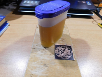
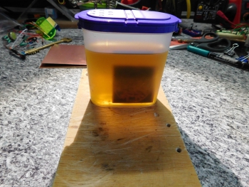
When all the powder has dissolved and the solution has acquired a uniform color, you can throw the board in there. It is desirable that the board floats on the surface, copper side down. Then the sediment will fall to the bottom of the container without interfering with the etching of the deeper layers of copper.
To prevent the board from sinking, you can double sided tape stick a piece of foam plastic to it. That's exactly what I did. It turned out very convenient. I screwed in the screw for convenience, so that I could hold it like a handle.
It is better to dip the board into the solution several times, and lower it not flat, but at an angle, so that no air bubbles remain on the surface of the copper, otherwise there will be jambs. Periodically you need to remove it from the solution and monitor the process. On average, etching a board takes from ten minutes to an hour. It all depends on the temperature, strength and freshness of the solution.
The etching process accelerates very sharply if you lower the hose from the aquarium compressor under the board and release bubbles. The bubbles mix the solution and gently knock out the reacted copper from the board. You can also shake the board or container, the main thing is not to spill it, otherwise you won’t be able to wash it off later.
When all the copper has been removed, carefully remove the board and rinse it under running water. Then we look at the clearing so that there is no snot or loose grass anywhere. If there is snot, then throw it into the solution for another ten minutes. If the tracks are etched or breaks occur, it means the toner is crooked and these places will need to be soldered with copper wire.

If everything is fine, then you can wash off the toner. For this we need acetone - the true friend of a substance abuser. Although now it is becoming more difficult to buy acetone, because... Some idiot from the state drug control agency decided that acetone is a substance used to prepare narcotics, and therefore its free sale should be prohibited. It works fine instead of acetone 646 solvent.

Take a piece of bandage and thoroughly moisten it with acetone and begin to wash off the toner. There is no need to press hard, the main thing is not to mess around too quickly so that the solvent has time to be absorbed into the pores of the toner, corroding it from the inside. It takes about two to three minutes to wash off the toner. During this time, even the green dogs under the ceiling will not have time to appear, but it still won’t hurt to open the window.
The cleaned board can be drilled. For these purposes, I have been using a motor from a tape recorder, powered by 12 volts, for many years. It’s a monster machine, although its lifespan lasts for about 2000 holes, after which the brushes burn out completely. You also need to rip out the stabilization circuit from it by soldering the wires directly to the brushes.

When drilling, you should try to keep the drill strictly perpendicular. Otherwise, then you’ll put a microcircuit in there. And with double-sided boards, this principle becomes basic.

The manufacture of a double-sided board occurs in the same way, only here three reference holes are made, with the smallest possible diameter. And after etching one side (at this time the other is sealed with tape so that it does not get etched), the second side is aligned along these holes and rolled. The first one is sealed tightly with tape and the second one is etched.
On the front side you can use the same LUT method to apply the designation of radio components for beauty and ease of installation. However, I don’t bother that much, but comrade Woodocat from the LJ community ru_radio_electr He always does this, for which I have great respect!
Soon I will probably also publish an article on photoresist. The method is more complicated, but at the same time it gives me more fun to do - I like to play tricks with reagents. Although I still make 90% of the boards using LUT.
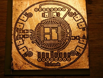
By the way, about the accuracy and quality of boards made using the laser ironing method. Controller P89LPC936 in the case TSSOP28. The distance between the tracks is 0.3mm, the width of the tracks is 0.3mm.

Resistors on the top size board 1206 . What's it like?
This video lesson shows the implementation of LUT technology, which is used to make a double-sided printed circuit board. At home you can make compact ones using SMD elements. Here's an example charger For lithium ion battery 18650 taken from an old laptop battery, we let's walk the path creating a board from printing the drawing to switching it on.
Watch the compressedvideo channel video
First of all, we draw a printed circuit board in the Eagle program for its subsequent manufacturing using laser-iron technology. About high-power lasers. The program is free for one- and two-sided applications. We upload each side of the signet in black and white into a graphic editor and combine them to print on one sheet. We will print on tracing paper. But to prevent the printer from jamming it, you will need glue and an A4 sheet. We buy 40 sheets of tracing paper at the nearest stationery store.
First, look for the smooth side. We take out a sheet of paper and check where it slides more than usual, this is the top side. Now we bend the sheet of paper so that we can insert tracing paper. 1-1.5 cm is enough. We do not coat it too much with glue, as it will go inside the printer, and we glue the tracing paper evenly. If you make it crooked, the two sides won't match.
Preparing a “sandwich”. Now we fold the sheet at the top to place it in a manual feed printer. Insert with tracing paper facing up. We get a fingerprint. We cut out a large piece and fold it along the fold, aligning the two sides of the board to the light. Tracing paper is ideal for this. All holes are visible and can be accurately aligned. We glue the sheet together to make a pocket, and we will place the board in it. To do this, coat it with glue on both sides.
Preparing a board for implementing LUT technology
To prepare the board we will need cleaning powder. If it says it cleans copper, that's it. You can take another one, or even paste. GOI (but not sandpaper). We take the powder and begin to clean the board until it reaches a mirror shine. Once there are no dark spots left on the board, it can be placed in the pocket. Once cleaned, you can only pick it up by the edges so as not to leave greasy fingerprints.
We place the board in the finished pocket and align it so that the entire print falls on it. Everything is ready for ironing. It is better to take a simple one without steam. Temperature at maximum. We carefully begin to iron over the entire area. The tracing paper sticks to the board and you can clearly see how the toner darkens. You don’t have to press too hard, but you need to iron both sides. Gradually the toner darkens and begins to bleed through the tracing paper. Once this has happened, everything is ready for the next operation. It is important not to overdo it, because the toner may spread and bottlenecks between the tracks may be flooded and will have to be cleaned up.
Now the tracing paper needs to be washed off. The toner will remain on the board, the paper will gradually come off. We cut it so that it all fits in the bath. We take ordinary water and throw the board there. We wait until it gets wet. After some time, the tracing paper begins to bubble and can be carefully removed. When wet, it comes off the board easily. The toner remains, covering all areas that we need to leave unetched. The tracing paper curls into lumps and gets wet. As a result, we get a beautiful, almost factory board.
It looks like it’s ready, but let’s take a magnifying glass and check how it turned out. It is clearly visible that there are pieces of paper left. The board will not be etched in these places. You need to remove the paper between the tracks. To do this we use a bristle brush. Moving along the paths, so as not to damage them, remove the remaining paper. When the board is dry, the places where the tracing paper remains are clearly visible, but this is not critical here. We drill a couple of holes on the side to insert the wire. She will help hold the board while we poison. We use ammonium persulfate. This is a rather aggressive substance and it is not recommended to dip your fingers in it. We take hot water from the tap. We dose it like this: one tablespoon of water per one teaspoon without a slide of persulfate. 5 spoons are enough for such a board. A water bath is also needed because the etching reaction actively cools the solution.
Stir with a plastic or glass rod. And remember that if the solution gets on your clothes, it will leave holes. Place the board in the solution and stir for about five minutes. At first the solution is transparent, then gradually turns blue. This copper goes into solution in the form of copper sulfate. We see that the copper has brightened. There is very little left until it completely disappears. The layer is very thin and it will disappear now.
After about five minutes, the board is cleaned, there are small spots left that need to be cleaned with a brush to speed up the process. Using a soft brush, remove any remaining copper.

The metal tip is wrapped with electrical tape to prevent it from being etched. We take white spirit, which dissolves printer toner well. We need to clean the board to prepare it for tinning. You can also clean with acetone or use nail polish remover. After washing off the toner, the resulting product shines with copper traces.
Tinning
We will tin with Rose alloy. To do this, we need a ladle, which will be damaged and no longer suitable for anything. A little citric acid, gloves, tweezers and the alloy itself. Rose has a melting point of just under 100 degrees. It consists of small granules, one of which is enough to tinning a board. Add a spoonful of citric acid and a few tablespoons of salt. And we boil it. We throw a grain of alloy onto the board.
Rose, if the temperature is sufficient, will melt. We try to smear it with a cotton swab. If it doesn’t melt, then you need to add more salt to raise the boiling point. The alloy should spread easily and effortlessly thin layer. We spread the alloy without lumps so that SMD elements can easily become. Now, within the framework of LUT technology, you can proceed to the next stage.
Drilling the board
Let's start drilling. A high-speed mini drill with a collet clamp was used. It allows you to clamp drills without distortion. Drills with a thicker shank are better. Drills of two sizes 0.5 and 0.8 are used; they can be taken for one size of collet clamp. It is better if you use a machine, but you can also carefully drill with a drill, it must be held strictly vertically. Then the holes on the top and bottom sides will fit exactly into the track seats. After drilling, you can make sure that both sides match perfectly.
Cutting the board
Now you can use regular metal scissors to cut the board to size. This can only be done if it is thin enough. The board is ready for soldering. To solder SMD elements, you need a special paste SOLDER PASTE, W001 is used, which is usually sold in tubes. Don't forget to store it in the refrigerator. We carry out soldering with a soldering hair dryer. Apply a drop of solder paste to each soldering point. Just a little bit is needed. If you don't have a needle, you can do this with a regular toothpick. A small drop is enough for soldering; if there are too many, you can end up shorting adjacent tracks. 
Parts distribution
We put the details in place. You can arrange them roughly, but make sure they stay on the paste. When soldering, they are aligned using surface tension forces. Special attention– microcircuits – they need to be placed more precisely. They, of course, also level out. But if they are placed crookedly, then you can get a short circuit in the tracks and either resolder them or remove the resulting “snot” with a soldering iron.
For our paste, a temperature of 230 degrees is enough; we set the minimum airflow so as not to blow our parts off the board. Heat each part until the solder melts. We see that the parts are aligned in place. Soldering with a hairdryer is a pleasure. It takes a long time to prepare, but the soldering itself is quick and high quality. In this case, you can solder the entire side of the board at a time. As a result, it turns out much faster than with a soldering iron.
Now the hardest part, three output parts that also need to be soldered, the rest are already in place. Before soldering the LEDs, it is a good idea to check their polarity. We switch the tester to the diode testing mode and, by the glow of the LED, determine where the plus and minus are. Let's take a tuning resistor, install it in place and solder it using a soldering iron. Since the board is double-sided, it is necessary to solder on both sides. The pins of the parts were also used to transmit a signal between the parties.
For convenience, it is better to use a “third hand” card holder, but you can do it without it, although it is less convenient. The result is this board for charging the battery, made using LUT technology. It is double-sided, there are both SMD and lead parts. Just look what convenient thing.
http//journal.caseclub.ru
Terms on specific example. For example, you need to make two boards. One is an adapter from one type of case to another. The second is replacing a large microcircuit with a BGA package with two smaller ones, with TO-252 packages, with three resistors. Board sizes: 10x10 and 15x15 mm. There are 2 options for manufacturing printed circuit boards in: using photoresist and the “laser iron” method. We will use the “laser iron” method.
The process of making printed circuit boards at home
1. Preparing a printed circuit board design. I use the DipTrace program: convenient, fast, high quality. Developed by our compatriots. Very convenient and pleasant user interface, unlike the generally accepted PCAD. There is a conversion to PCAD PCB format. Although many domestic companies have already begun to accept DipTrace format.
In DipTrace you have the opportunity to see your future creation in volume, which is very convenient and visual. This is what I should get (the boards are shown in different scales):

2. First, we mark the PCB and cut out a blank for the printed circuit boards.


4. Don’t forget to clean and degrease the board blank. If you don’t have a degreaser, you can go over the copper of the fiberglass with an eraser. Next, using an ordinary iron, we “weld” the toner from the paper to the future printed circuit board. I hold it for 3-4 minutes under slight pressure until the paper turns slightly yellow. I set the heat to maximum. I put another sheet of paper on top for more uniform heating, otherwise the image may “float”. Important point here - uniformity of heating and pressure.


5. After this, after allowing the board to cool a little, we place the workpiece with the paper stuck to it in water, preferably hot. Photo paper quickly gets wet, and after a minute or two you can carefully remove the top layer.


In places where there is a large concentration of our future conductive paths, the paper to the board is especially strong. We're not touching it yet.

6. Let the board soak for a couple more minutes. Carefully remove the remaining paper using an eraser or rubbing with your finger.


7. Take out the workpiece. Dry it. If somewhere the tracks are not very clear, you can make them brighter with a thin CD marker. Although it is better to ensure that all tracks are equally clear and bright. This depends on 1) the uniformity and sufficient heating of the workpiece with the iron, 2) accuracy when removing the paper, 3) the quality of the PCB surface and 4) successful selection of paper. You can experiment with the last point to find the most suitable option.


8. Place the resulting workpiece with future conductor tracks printed on it in a ferric chloride solution. We poison for 1.5 or 2 hours. While we wait, let’s cover our “bath” with a lid: the fumes are quite caustic and toxic.


9. We take the finished boards out of the solution, wash and dry. The toner is easily washed off the board using acetone. As you can see, even the thinnest conductors with a width of 0.2 mm came out quite well. There is very little left.

10. We tin the printed circuit boards made using the “laser iron” method. We wash off the remaining flux with gasoline or alcohol.

11. All that remains is to cut out our boards and mount the radio elements!
conclusions
With some skill, the “laser iron” method is suitable for making simple printed circuit boards at home. Short conductors from 0.2 mm and wider are quite clearly obtained. Thicker conductors turn out quite well. Time for preparation, experiments with selecting the type of paper and iron temperature, etching and tinning takes approximately 3-5 hours. But it’s much faster than ordering boards from a company. Cash costs are also minimal. In general, for simple budget amateur radio projects, the method is recommended for use.